
Motorola 68040
First 680x0 with on-chip FPU and MMU; used in Mac Quadra.

Konstantin Lanzet · CC BY-SA 3.0
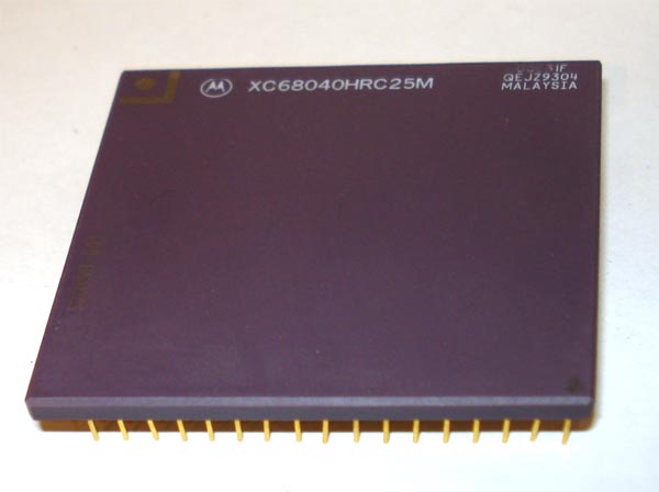
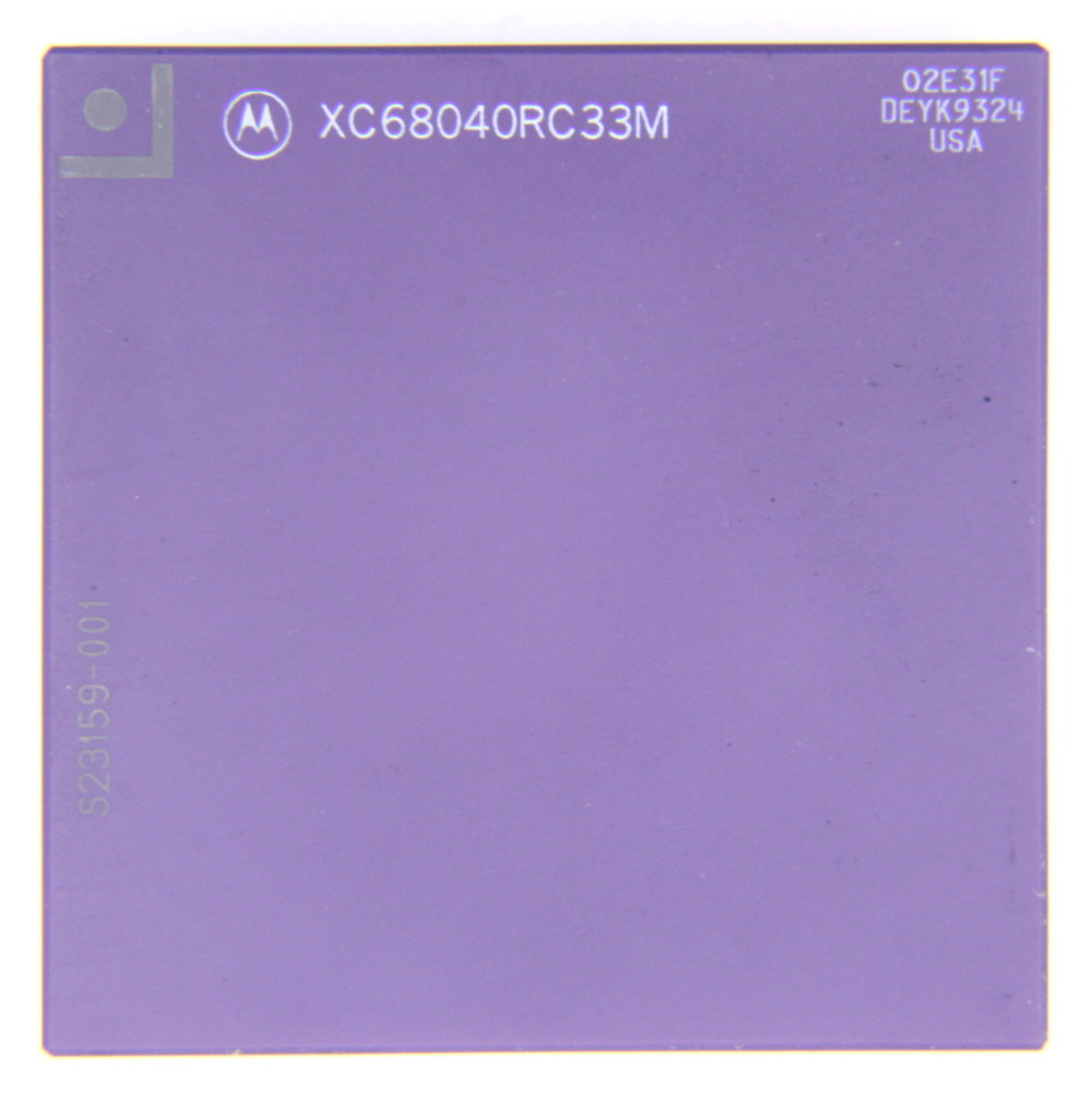
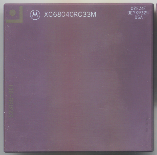
The Motorola 68040 (pronounced "sixty-eight-oh-forty" and often referred to as the '040) is a 32-bit microprocessor in the Motorola 68000 series. Previewed in April 1989, announced in January 1990, and available in limited volumes from late 1990, it succeeded the 68030 and was followed by the 68060, skipping the 68050. It was the first 680x0 family member with an on-chip Floating-Point Unit (FPU), integrating all functionality that previously required external chips: the FPU and the Memory Management Unit (MMU, added in the 68030). It also featured split instruction and data caches of 4 kilobytes each and a fully pipelined six-stage design.
Quick Facts
- Designfirm
- Motorola
- Produced-Start
- 1990
- Arch
- Motorola 68000 series
- Data-Width
- 32 bits
- Slowest
- 25
- Slow-Unit
- MHz
- Fastest
- 40
- Transistors
- ~1,200,000
- Variant
- 68LC040 and 68EC040
- Predecessor
- Motorola 68030
- Successor
- Motorola 68060
Facts from the source article.
Lore & Background
The 68040 ran into the transistor budget early in design. While the MMU did not take many transistors—indeed, having it on the same die as the CPU saved transistors—the FPU certainly did. Motorola's 68882 external FPU was known as a very high performance unit, and Motorola did not wish to risk integrators using the "LC" version with a 68882 instead of the more profitable full "RC" unit. The FPU in the 68040 was incapable of IEEE transcendental functions, which had been supported by both the 68881 and 68882 and were used by popular fractal generating software of the time and little else. The Motorola floating-point support package (FPSP) emulated these instructions in software under interrupt; heavy use caused severe performance penalties.
Heat was always a problem throughout the 68040's life. While it delivered over four times the per-clock performance of the 68020 and 68030, the chip's complexity and power requirements came from a large die and large caches. This affected scaling, and it was never able to run with a clock rate exceeding 40 MHz. A 50 MHz variant was planned but canceled. Overclocking enthusiasts reported success reaching 50 MHz using a 100 MHz oscillator instead of an 80 MHz part and the then novel technique of adding oversized heat sinks with fans.
The 68040 offered the same features as the 80486, but on a clock-for-clock basis could significantly outperform the Intel chip in integer and floating-point instructions according to Motorola's own benchmark results. Independent measurements of floating-point performance in workstation systems suggested rather more modest gains over the 80486 and SPARC in Motorola's chosen LINPACK benchmark, largely confined to double-precision operations. Vendor literature such as that describing the NeXTstation Color and Turbo Color models advertised somewhat lower ratings than Motorola's own literature. However, the 80486 could be clocked significantly faster without overheating problems and quickly spawned a mobile derivative for laptops.
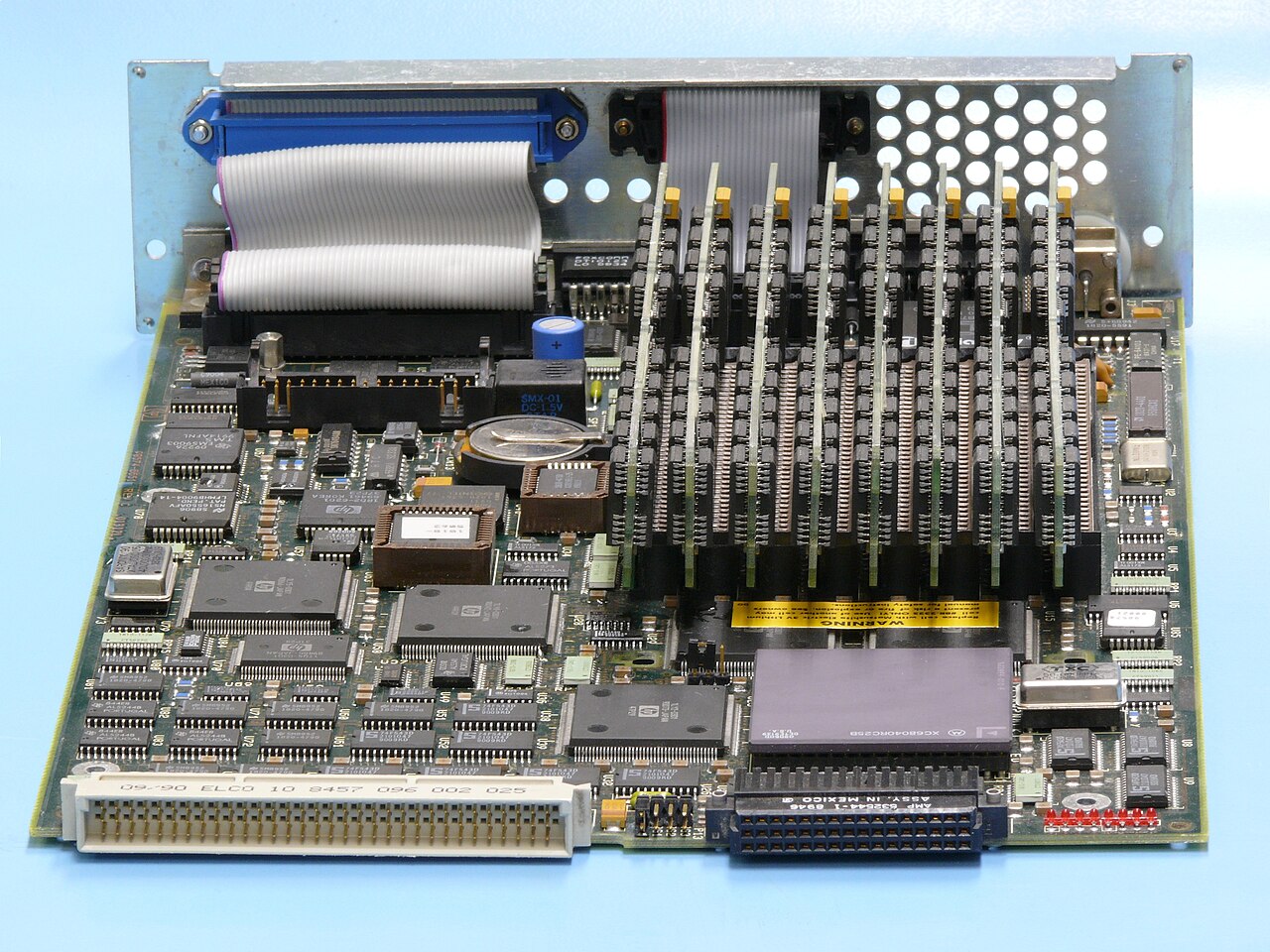
Reader's Guide
The 68040's significance lies in its integration of the FPU and MMU on a single die, making it a complete single-chip microprocessor for its era. It was used in Apple Macintosh Quadra computers (named for the chip), with the fastest 40 MHz version appearing only in the Quadra 840AV. The 68LC040 (no FPU) appeared in cheaper Quadra, Centris, Performa, and some late-model LC Macs. Beyond Apple, it powered the Amiga 4000 and 4000T, workstations such as the HP 9000/400 series and NeXT computers, Alpha Microsystems servers, NCR TOWER systems, and Apollo Computer's DN5500. Its legacy extends to embedded and safety-critical roles: the 68040 processor is used in flight management computers aboard many Boeing 737 aircraft (including all Next Generation and MAX models) and in the flight control system of the Saab JAS 39 Gripen. The 68EC040 variant (no FPU, no MMU) was used in Cisco switch Supervisor Engine I for models including the 2900, 4000, 5000, 6000, 6500, and 7600. A bug in some 68LC040 mask revisions caused loss of pending writes when an F-line exception was triggered, affecting software FPU emulation; this was fixed in mask set 2E71M or later, introduced in mid-1995.
Did You Know?
- A planned 50 MHz variant was canceled due to exceeding the thermal design envelope.
- The 68LC040 variant removed the FPU; the 68EC040 removed both FPU and MMU.
- The 68040 is used in flight management computers aboard Boeing 737 Next Generation and MAX models.
Integrated Architecture and the Transistor Budget
The 68040 marked a turning point in the 680x0 family by bringing both the floating-point unit and the memory management unit onto a single die. Previously, the FPU had lived on a separate chip, and the MMU had been added as a discrete component back in the 68030 era. By consolidating these blocks, Motorola eliminated the need for external companion chips, though the design immediately ran into transistor-count constraints. The FPU consumed a substantial share of the available silicon, and the resulting unit dropped support for IEEE transcendental functions that both the 68881 and 68882 had handled natively. Motorola's floating-point support package emulated those instructions through a software interrupt handler, which imposed significant performance hits whenever fractal-generation or similar workloads exercised them heavily. The chip also featured separate four-kilobyte instruction and data caches alongside a six-stage pipeline. Motorola's decision to integrate the FPU was partly commercial: they feared that integrators would pair the cheaper LC variant with the standalone 68882, undermining sales of the more profitable full RC part.
Market Segments and the Variant Family
Motorola carved the 68040 into distinct product tiers to serve different price and power requirements. The 68LC040 stripped out the FPU while retaining the on-chip caches and six-stage pipeline, making it meaningfully faster than a 68030 despite resembling one on a feature chart. The 68EC040 went further, removing both the FPU and the MMU to cut cost and power draw for embedded controllers; it found a home in Cisco's Supervisor Engine I across a wide range of switch models. Ironically, the embedded market of the early 1990s rarely demanded 68040-level performance, so older EC variants of the 68020 and 68030 remained the workhorses in those designs. Speed grades ranged from 25 MHz and 33 MHz across the full line to a 40 MHz part reserved for the complete 68040 until roughly 2000. The 16 and 20 MHz grades existed only as unqualified prototyping samples. Pricing started at a reported $795 per unit at the January 1990 announcement, dropped to $595 for volume production later that year, and reached $337 for the 25 MHz part by late 1992, nearly matching Intel's 33 MHz 80486DX at $328.
From Workstations to Cockpits
The 68040 found its most visible home in Apple's Macintosh Quadra line, a product family literally named after the chip. The top-of-the-line Quadra 840AV was the only Mac to use the full 40 MHz 68040, while pricier models in the short-lived Centris series also adopted the processor. Budget-oriented Quadra, Centris, Performa, and late-model LC machines instead shipped with the 68LC040. Beyond Apple, the chip powered the Amiga 4000 and 4000T, a spread of professional workstations from Alpha Microsystems, the HP 9000/400 series, NCR's TOWER 32/750, 32/825, and 32/850, Apollo Computer's DN5500, and later revisions of the NeXT computer. Perhaps most strikingly, the 68040 earned a place in critical aviation systems: it serves as the processor in the flight management computers aboard Boeing 737 Next Generation and MAX aircraft, and it underpins the flight control system of the Saab JAS 39 Gripen fighter jet. These deployments speak to the chip's reliability and real-time performance characteristics in safety-critical environments.
Heat, Speed, and the Rivalry with Intel
Despite delivering more than four times the per-clock throughput of the 68020 and 68030, the 68040 was chronically constrained by thermal limits. Its large die and generous caches generated significant heat, capping the practical clock speed at 40 MHz. A planned 50 MHz grade was scrapped after it breached the thermal design limits, though overclocking enthusiasts eventually coaxed 50 MHz out of the chip by substituting a 100 MHz oscillator for the standard 80 MHz part and bolting on oversized heat sinks with active cooling. In head-to-head comparisons with Intel's 80486, Motorola's own benchmarks claimed clear wins in both integer and floating-point throughput, but independent workstation measurements painted a more modest picture, with advantages largely confined to double-precision floating-point work. Crucially, the 80486 could be clocked considerably higher without thermal collapse and quickly spawned a mobile derivative for laptops. This gap left Apple stranded: the 100-series PowerBook launched in 1992 still relied on the aging 68030, and a 68040-equipped laptop did not arrive until the PowerBook Duo 280 and 500 series in 1994.
Gallery
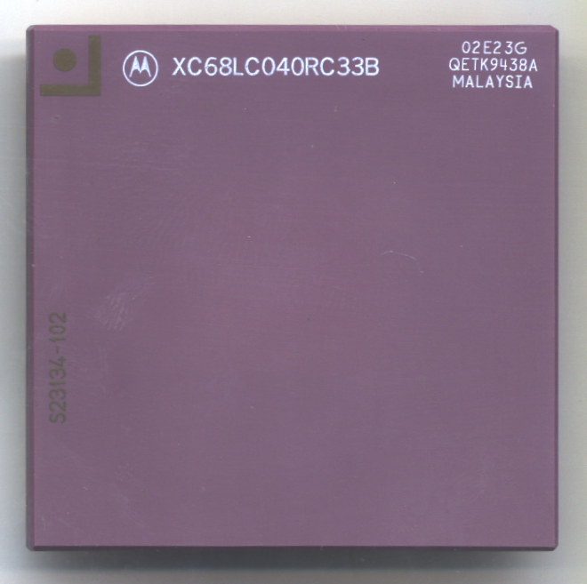
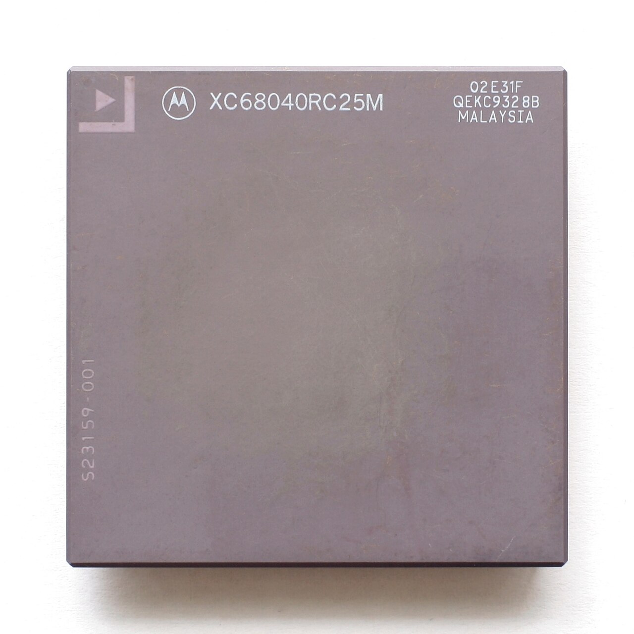
Frequently Asked Questions
What is the Motorola 68040?
The 68040, commonly nicknamed the "'040," is a 32-bit CPU in Motorola's 68000 family of microprocessors. It occupies the slot between the 68030 and the 68060, with the 68050 number simply left unused.
What made the 68040 stand out from earlier 680x0 chips?
It was the first 680x0 to integrate both a floating-point unit and a memory management unit directly onto the die, removing the need for separate coprocessor chips. The chip also shipped with 4 KB split instruction and data caches plus a six-stage pipeline.
When did the Motorola 68040 actually become available?
Motorola previewed the part in April 1989 and gave its official announcement in January 1990, but limited production volumes did not reach customers until late 1990.
What was the Motorola 68040 used in?
The '040 found its most prominent home in Apple's Macintosh Quadra line, where its built-in FPU and MMU helped drive professional and power-user workstations.
Why is the Motorola 68040 considered important?
By folding the FPU and MMU onto a single die, the '040 simplified system design and lowered the cost of 32-bit protected-mode computing. It also set the architectural groundwork for the 68060, making it a pivotal link in Motorola's 68000 lineage.
More in Microprocessors, Part 3 1-24
Spotted an error? Know more?
Reader corrections go straight into our review queue. Suggest an edit · How this site is sourced