
Intel i860
Intel's first million-transistor RISC chip with VLIW architecture.

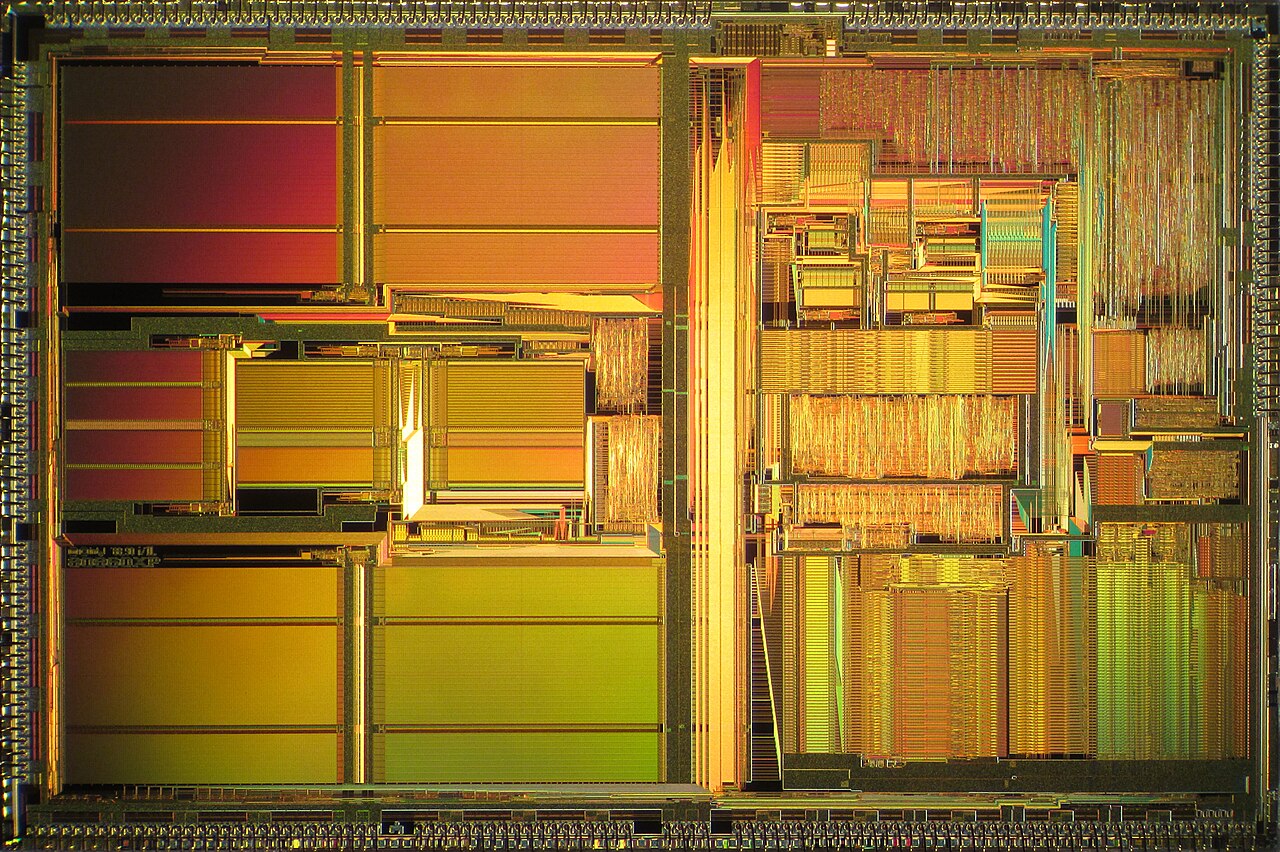
ZyMOS · CC BY-SA 4.0
The Intel i860 (or 80860) was a RISC microprocessor that Intel launched in 1989. It marked one of the company's first major pushes into a brand-new, high-end instruction set architecture after the earlier iAPX 432 had flopped in the early 1980s. This chip also held the distinction of being the first commercially available microprocessor to pack one million transistors. Despite a highly publicized debut—which somewhat overshadowed the earlier i960, a chip that found steady success in certain embedded markets—the i860 never took off commercially, and Intel pulled the plug on the project by the mid-1990s.
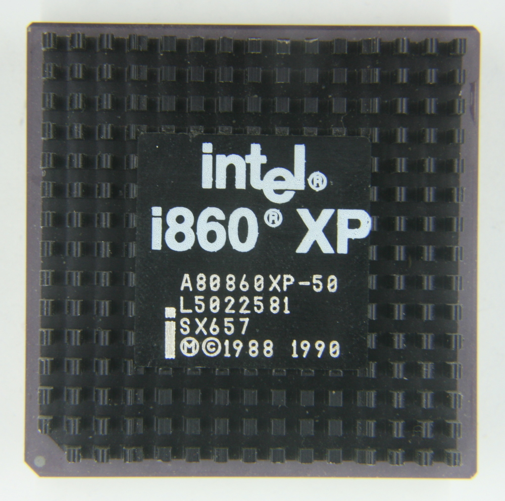
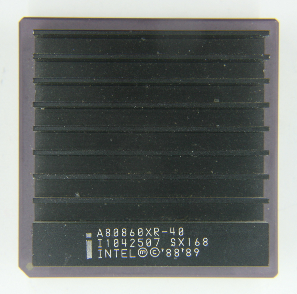
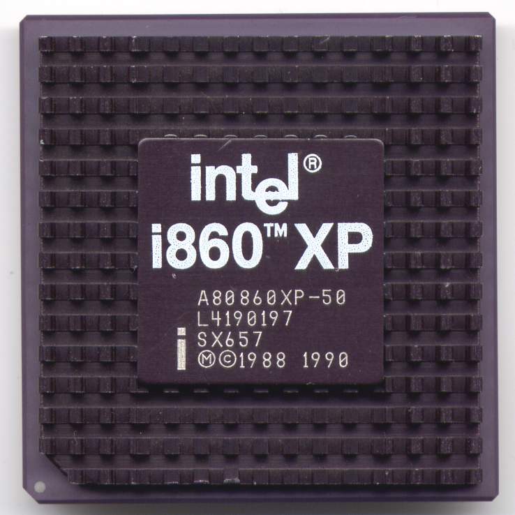
The first implementation, the i860 XR (codenamed N10), ran at 25, 33, or 40 MHz. (Microsoft engineers later coined the name "NT" from the chip's codename, "N-ten.") The second-generation i860 XP (codenamed N11) added support for 4 MB memory pages, larger on-chip caches, a second-level cache interface, faster buses, and hardware bus snooping for cache coherence in multiprocessor setups. A die shrink from 1 µm to 0.8 µm using Intel's CHMOS V process boosted clock speeds to 40 and 50 MHz. Both chips shared the same instruction set for application software.
The i860 packed several then-unique features, most notably a very long instruction word (VLIW) architecture and robust support for high-speed floating-point math. Its design split instructions into two classes: "core" instructions, which used a 32-bit ALU, and "floating-point or graphics" instructions, which targeted a floating-point adder, a floating-point multiplier, or a 64-bit integer graphics unit. Separate pipelines existed for the ALU, floating-point adder, floating-point multiplier, and graphics unit. The chip could fetch and decode one core instruction and one floating-point/graphics instruction per clock cycle. Using dual-operation floating-point instructions—which passed values between consecutive dual-operation instructions—it could execute up to three operations per cycle (one ALU, one floating-point multiply, and one floating-point add or subtract).
All data buses were at least 64 bits wide; the internal memory bus to the cache was 128 bits wide. Core instructions used thirty-two 32-bit integer registers.
Quick Facts
- Designer
- Intel
- Bits
- 32/64-bit
- Introduced
- 1989
- Design
- RISC, VLIW
- Encoding
- Fixed
- Branching
- Compare and branch
- Endianness
- Bi (switchable)
- Page Size
- 4 KB
- Extensions
- 64-bit graphics unit
- Gpr
- 32 32-bit
- Fpr
- 32 32-bit (16 64-bit)
Facts from the source article.
Lore & Background
The i860 combined a number of features that were unique at the time, most notably its very long instruction word (VLIW) architecture and powerful support for high-speed floating-point operations. The design used two classes of instructions: 'core' instructions using a 32-bit ALU, and 'floating-point or graphics' instructions operating on a floating-point adder, a floating-point multiplier, or a 64-bit integer graphics unit. It could fetch and decode one core instruction and one floating-point or graphics instruction per clock, and with dual-operation floating-point instructions could execute up to three operations per clock. All data buses were at least 64 bits wide, and the internal memory bus to the cache was 128 bits wide.
The first implementation was the i860 XR (code-named N10, after which Microsoft's engineers coined the name 'NT' for N-ten), running at 25, 33, or 40 MHz. The second-generation i860 XP (code-named N11) added 4 Mbyte pages, larger on-chip caches, second-level cache support, faster buses, and hardware support for bus snooping for cache coherence in multiprocessor systems. A process shrink from 1 μm to 0.8 μm using the CHMOS V process increased the clock to 40 and 50 MHz. Both microprocessors supported the same instruction set for application programs.
The i860 had both non-delayed and delayed branch instructions, with a single branch delay slot. The pipelines into the functional units were program-accessible (VLIW), requiring compilers to order instructions carefully in the object code to keep the pipelines filled. This was an attempt to move scheduling off-chip into the compiler, allowing more room for functional units. As a result, the i860 could run certain graphics and floating-point algorithms with exceptionally high speed, but its performance in general-purpose applications suffered and it was difficult to program efficiently.
Reader's Guide
The i860's significance lies in its pioneering VLIW architecture and its role as Intel's first million-transistor chip, but its legacy is largely one of commercial failure. On paper, performance was impressive for a single-chip solution, but real-world performance was poor. Runtime code paths were difficult to predict, making it exceedingly hard for compilers to order instructions properly at compile time. If an incorrect guess was made about data being in cache, the entire pipeline would stall. While theoretically capable of peaking at about 60-80 MFLOPS for the XP versions, manually written assembler code managed only about 40 MFLOPS, and most compilers had difficulty getting even 10 MFLOPS. The later Itanium architecture, also a VLIW design, suffered again from the problem of compilers incapable of delivering sufficiently optimized code.
Another serious problem was the lack of any solution to handle context switching quickly. An interrupt could spill the several pipelines and require them all to be re-loaded, taking 62 cycles in the best case and almost 2000 cycles in the worst—up to 50 microseconds at 40 MHz, an eternity for a CPU. This largely eliminated the i860 as a general-purpose CPU. As compilers improved, general performance did likewise, but by then most other RISC designs had already passed the i860. Andy Grove suggested the failure was due to Intel being stretched too thin. The i860 saw some use in supercomputers, workstations, and as a graphics accelerator, but these uses slowly disappeared as more general-purpose CPUs matched its performance and Intel turned its focus to Pentium processors.
Did You Know?
- The i860 was the world's first million-transistor chip.
- Microsoft's engineers coined the name 'NT' from the i860 XR's code-name N10.
- The i860 could execute up to three operations per clock using dual-operation floating-point instructions.
- The i860's graphics unit supported SIMD-like instructions that influenced Intel's later MMX functionality.
Architecture & Design Philosophy
The i860 represented a bold departure from conventional microprocessor design, built around a very long instruction word philosophy that placed the burden of instruction scheduling squarely on the compiler rather than on-chip hardware. The chip organized its operations into two distinct instruction classes: a core class driving a 32-bit integer ALU, and a floating-point or graphics class feeding a dedicated adder, multiplier, and a 64-bit integer graphics unit. Each of these functional units received its own pipeline, and the architecture allowed the processor to fetch and decode one instruction from each class per clock cycle. In dual-operation mode, the instruction cache was accessed as paired 64-bit words, enabling up to three simultaneous operations—one ALU, one floating-point multiply, and one floating-point add or subtract. All external data buses were at least 64 bits wide, while the internal path to cache stretched to 128 bits. The core register file held thirty-two 32-bit integer registers, while the floating-point and graphics register file could be viewed as thirty-two 32-bit, sixteen 64-bit, or eight 128-bit floating-point slots, or sixteen 64-bit integer slots for graphics work. Branch handling included both non-delayed and delayed forms, with a single delay slot in the latter case.
The Compiler's Burden and Performance Reality
On paper, the i860's dual-pipeline design promised extraordinary throughput, yet in practice the chip's performance fell dramatically short of its theoretical ceiling. The fundamental problem was that the VLIW architecture demanded the compiler perfectly sequence instructions to keep every pipeline saturated, a task that proved nearly impossible when runtime behavior—such as whether data resided in cache—could not be predicted at compile time. A single cache miss would stall the entire pipeline, and the compiler had no mechanism to adapt. The XP revision was theoretically capable of 60 to 80 megaflops in both single and double precision, but hand-tuned assembler code reached only around 40 megaflops, and most compilers struggled to extract even 10. Compounding the issue, context switching was catastrophically slow: an interrupt could spill all pipelines, requiring 62 cycles in the best case and nearly 2,000 in the worst—roughly 50 microseconds at 40 MHz, an eternity for a processor. This effectively disqualified the i860 as a general-purpose CPU, a fate that would later echo in Intel's Itanium, another VLIW design hamstrung by compilers unable to deliver sufficiently optimized code.
Two Generations of Silicon
Intel brought the i860 architecture to life in two successive microprocessor generations. The first, the XR (internally code-named N10), operated at 25, 33, or 40 MHz and carried the distinction of being the world's first million-transistor chip. The N10 codename was so memorable that Microsoft engineers borrowed the "N-ten" reference when naming their operating system NT. The second generation, the XP (code-named N11), expanded the design with 4-megabyte memory pages, larger on-chip caches, support for a second-level cache, faster external buses, and hardware-assisted bus snooping to maintain cache coherence across multiprocessor systems. A process shrink from 1 micrometer to 0.8 micrometer using Intel's CHMOS V fabrication process pushed the XP's clock speeds to 40 and 50 MHz. Despite these hardware differences, both generations shared an identical application-level instruction set. Intel marketed the chip as the "i860 64-Bit Microprocessor," emphasizing its wide datapaths, and the graphics unit offered SIMD-like operations that could pack multiple 8-bit, 16-bit, or 32-bit pixels into a single 64-bit integer lane.
A Short-Lived Ambition and Lasting Influence
The i860 launched in 1989 with considerable industry fanfare, a spectacle that somewhat overshadowed Intel's earlier i960, which had quietly found success in embedded-systems niches. The project represented one of Intel's first forays into an entirely new high-end instruction set since the ill-fated iAPX 432 of the early 1980s. Yet commercial traction never materialized, and the program was quietly terminated in the mid-1990s. By the time compilers matured enough to extract better performance from the VLIW pipelines, competing RISC designs had already surpassed the i860 in practical speed. In the late 1990s, Intel abandoned its entire RISC product line in favor of ARM-based processors branded as XScale. Nevertheless, the i860 left a tangible mark on Intel's future: the SIMD-style graphics instructions that let a 64-bit datapath process multiple pixels simultaneously directly informed the MMX technology later added to Pentium processors. The chip's cautionary tale about compiler-dependent performance also loomed over the Itanium project, which inherited the same VLIW scheduling challenges.
Gallery
Frequently Asked Questions
What is the Intel i860?
The i860 (also known as the 80860) was a RISC microprocessor that Intel shipped in 1989, representing one of the company's earliest serious bets on a high-end instruction set architecture outside its x86 family. It followed the commercial disappointment of the iAPX 432 in the early 1980s and signaled Intel's intent to compete in the emerging RISC market.
What made the Intel i860 historically notable?
The i860 was the first commercially available microprocessor to integrate one million transistors on a single die. It also employed a VLIW (Very Long Instruction Word) architecture, an unusual and ambitious design choice for a production chip of that era.
What were the i860's generations and clock speeds?
The first-generation i860 XR (code-named N10) was offered at 25, 33, and 40 MHz. The second-generation i860 XP (code-named N11) raised the ceiling to 40 or 50 MHz.
Why did the Intel i860 fail commercially?
Despite a heavily publicized 1989 launch that drew more headlines than the already-shipping i960, the i860 never found a meaningful market niche and failed to gain traction with system integrators. Intel ultimately discontinued the project in the mid-1990s.
How did the i860 relate to Intel's earlier i960?
The i960 had been shipping before the i860 and carved out a steady role in embedded and real-time applications. The i860 was positioned as the higher-performance successor, but its flashy debut inadvertently overshadowed the i960, which continued to serve its embedded niche while the i860 targeted the high-end segment it never captured.
More in Microprocessors, Part 3 1-24
Spotted an error? Know more?
Reader corrections go straight into our review queue. Suggest an edit · How this site is sourced