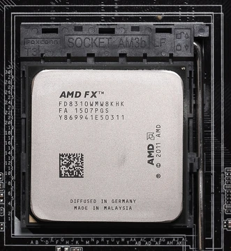
Intel microprocessor
Intel microprocessors span from the 4004 to modern multi-chip module designs.

Jacek Halicki · CC BY-SA 4.0
The Intel microprocessor is a series of central processing units (CPUs) introduced by Intel, beginning with the 4-bit 4004 in 1971. These processors have evolved through multiple generations, from early 8-bit designs to modern high-end offerings, including the latest Xeon 6+ and Core Series 3 announced in 2026.
- First commercially available microproces
- Intel 4004, introduced November 15, 1971
- Clock rate (4004)
- 740 kHz
- Transistors (4004)
- 2,300 at 10 μm
- Addressable memory (4004)
- 640 bytes
- Program memory (4004)
- 4 KB
- Latest release
- Xeon 6+ (Clearwater Forest), released at Computex 2026 on June 1, 2026
- Latest core series 3 announcement
- Panther Lake, announced at CES 2026 on January 5, 2026
Lore & Background
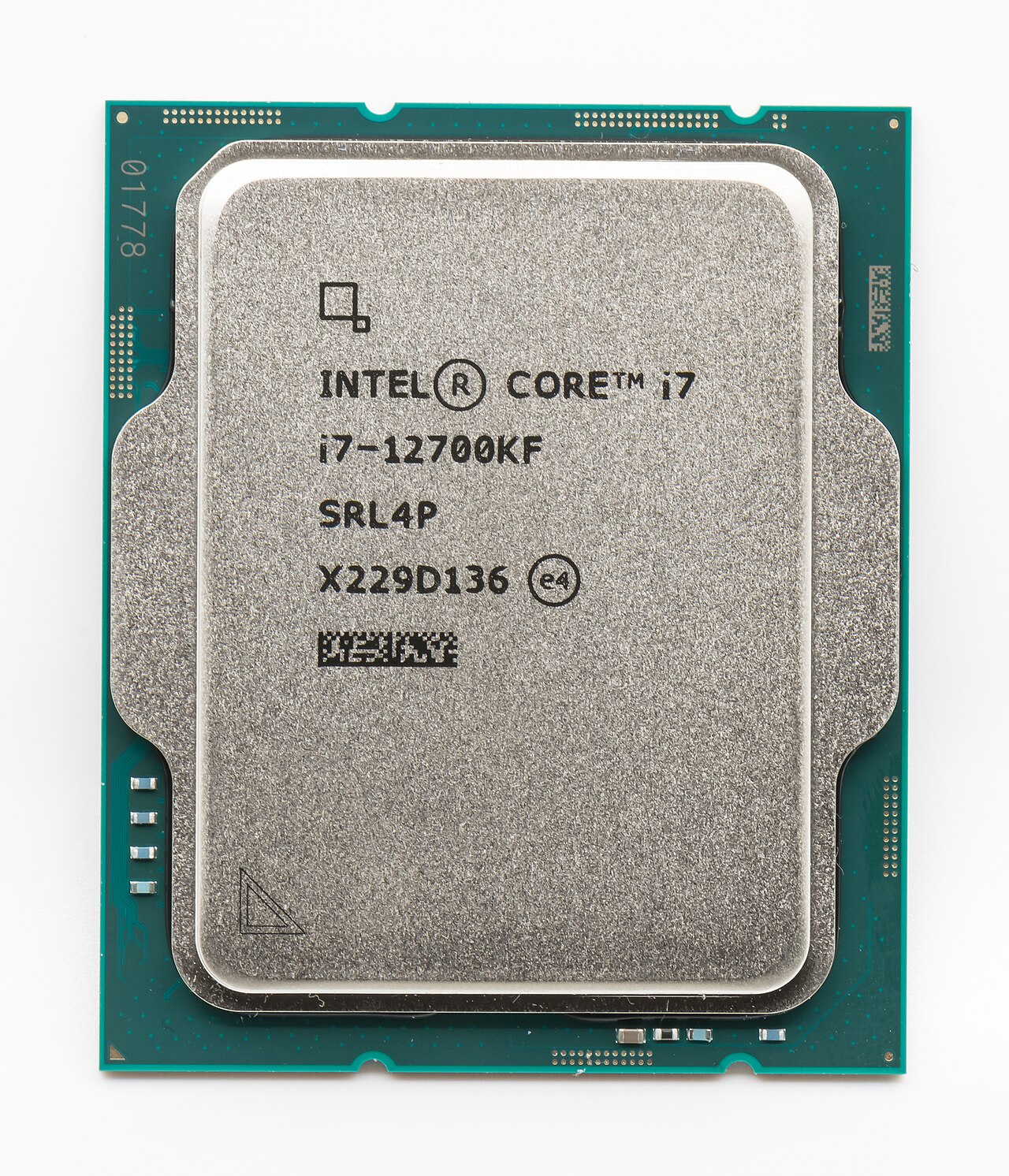
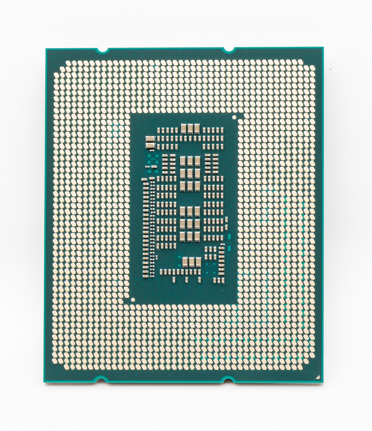
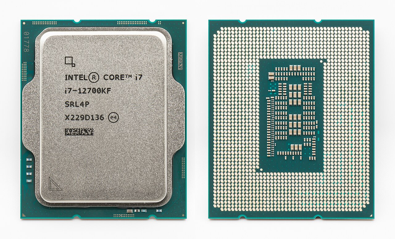
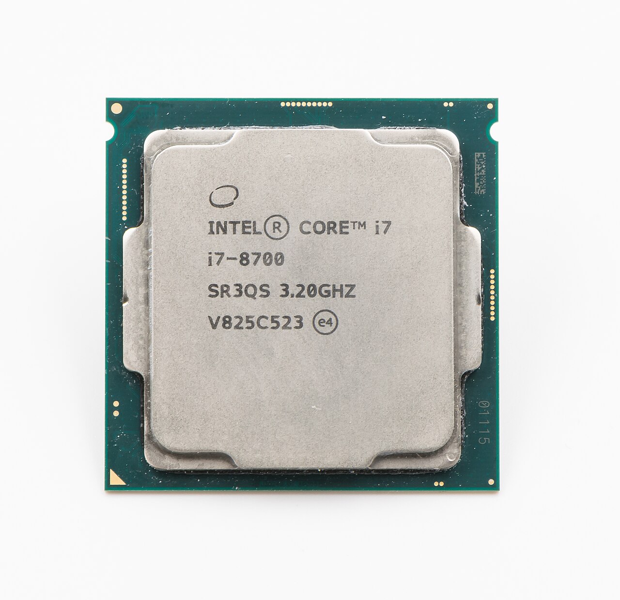
Intel's microprocessor line began with the 4004, the first commercially available single-chip IC processor, designed for the Busicom calculator. It was followed by the 4040 in 1974 and the 8008 in 1972, an 8-bit processor. The 8-bit processors used PMOS logic and had limited addressable memory. Over decades, Intel introduced generations such as the 6th (Skylake), 7th (Kaby Lake), 8th (Coffee Lake), 9th (Coffee Lake Refresh), 10th (Comet Lake, Ice Lake, Amber Lake), 11th (Rocket Lake and Tiger Lake), 12th, 13th, and 14th generation Core i processors, each with desktop and mobile variants. The 11th generation desktop processors were based on Rocket Lake, a 14nm backport of the 10nm Sunny Cove architecture, while mobile processors used Tiger Lake with the 10nm Willow Cove microarchitecture. The 12th generation introduced a hybrid design with P-Cores and E-Cores. Core Series 2, released on October 24, 2024, moved from monolithic silicon to a disaggregated MCM design, with Arrow Lake and Lunar Lake not supporting Hyper-Threading. Core Series 2 Plus (Arrow Lake Refresh) was released on March 26, 2026. Core Series 3 (Panther Lake) was announced at CES 2026, including mobile and handheld gaming processors. The Xeon 6+ (Clearwater Forest) was released at Computex 2026 on June 1, 2026, for network infrastructure and data center servers, supporting up to 1.5 TB of DDR5 RDIMM 8000MT/s RAM and ECC memory, and is E-Core only.
Reader's Guide
The Intel microprocessor's significance lies in its pioneering role as the first commercially available single-chip CPU, the 4004, which enabled the development of modern computing. Over generations, Intel introduced key architectural shifts, such as the move from monolithic to multi-chip module designs with Core Series 2, and the adoption of hybrid architectures combining P-Cores and E-Cores. The 11th generation saw a backport of a 10nm architecture to 14nm for desktop processors. The 12th generation introduced hybrid designs, while later generations like Core Series 2 and Core Series 2 Plus refined disaggregated designs. The Xeon 6+ targets data center and network infrastructure with high memory capacity and ECC support. The Core Series 3 extends into mobile and handheld gaming. Intel's branding evolved from Core i3/i5/i7/i9 to Core and Core Ultra with Meteor Lake. The legacy includes continuous innovation in process nodes, memory support, and feature sets such as Intel vPro, Intel Speed Select, and ECC memory support across various chipsets.
Did You Know?
- The Intel 4004 was the first commercially available microprocessor, introduced on November 15, 1971.
- The 4004 had 2,300 transistors at 10 μm and a clock rate of 740 kHz.
- The Xeon 6+ (Clearwater Forest), released June 1, 2026, supports up to 1.5 TB of DDR5 RDIMM 8000MT/s RAM.
Architecture and Performance Gains
The Intel 80286 represented a significant architectural leap over its 8086 predecessor, packing approximately 134,000 transistors into a 68-pin package available in PLCC, LCC, and PGA configurations. At its core, the chip organized its logic into four independent functional units—the address unit, bus unit, instruction unit, and execution unit—arranged in a loosely coupled buffered pipeline similar to the 8086's approach. However, the 286 introduced non-multiplexed address and data buses, a first in the 8086-based family, and a dedicated address calculation unit that handled base-plus-index operations without burdening the general-purpose ALU. This alone eliminated several wasted clock cycles that the older processor required. Combined with more efficient instruction prefetching, jump handling, and microcoded operations like MUL and DIV, the 286 delivered more than double the per-clock performance of the 8086 in many workloads. Typical throughput measured around 0.21 instructions per clock, with the 6, 10, and 12 MHz variants achieving roughly 0.9, 1.5, and 2.66 MIPS respectively.
Protected Mode and Memory Management
The 80286 made history as the first x86 processor to offer protected virtual-address mode and the first commercially available microprocessor with an on-chip memory management unit. Its 24-bit address bus expanded the physical address space to 16 megabytes, a sixteen-fold increase over the 8086's 1 megabyte limit, and it introduced virtual memory support of up to 1 gigabyte through segmentation. The protection model worked by dividing memory into distinct segments for code, data, and stack, each assigned a privilege level that prevented lower-privilege segments from accessing higher-privilege ones. A new set of instructions—ARPL, CLTS, LAR, LGDT, LIDT, LLDT, LMSW, LSL, LTR, SGDT, SIDT, SLDT, SMSW, STR, VERR, and VERW—gave operating systems the tools to manage this environment. One notable design constraint was that the processor could not exit protected mode back to real mode without a hardware reset. IBM addressed this in the PC/AT by adding external circuitry and specialized ROM BIOS code, along with 8042 keyboard controller routines, to permit a software-triggered reset that preserved active memory.
The PC/AT Era and Production Lifecycle
Although Intel initially envisioned the 80286 for industrial automation, transaction processing, and telecommunications rather than personal computers, it found its most famous home in the IBM PC/AT, launched in 1984. The chip became the standard processor in AT-compatible machines throughout the late 1980s and into the early 1990s, and by 1987 Intel had shipped its five-millionth unit. Production quality was not without challenges: the early B-step and C-step revisions, common in AT and AT-clone systems, carried several significant errata that frustrated programmers and operating-system developers. The E-stepping revision, available by late 1986, resolved these issues. Intel also second-sourced the design to Fujitsu around 1985, and fully static CMOS versions were developed by Intel as the 80C286, as well as by Intersil and Fujitsu, targeting battery-powered applications. Clock speeds began at 5, 6, and 8 MHz, rose to 12.5 MHz in later Intel releases, and eventually reached 16, 20, and 25 MHz through AMD and Harris. Despite its expanded 16-megabyte address space, memory costs meant most 286-based machines shipped with no more than 1 megabyte of RAM for much of its production run.
Intended Applications and Instruction Set
Intel's original marketing targeted the 80286 at multi-user environments: automated PBX systems, real-time process control, and transaction-processing hardware. The chip was engineered to support multitasking workloads, and its protected-mode capabilities were meant to let IBM-compatible machines compete in the Unix-dominated server and workstation market for the first time. The instruction set inherited everything from the 8086 and 8088, plus the additions from the 80186—ENTER, LEAVE, BOUND, INS, OUTS, PUSHA, POPA, immediate PUSH, IMUL with immediate operands, and immediate shifts and rotates. In the 80287 co-processor pairing, the 286 could handle unsigned packed decimal, unsigned binary, unsigned unpacked decimal, and signed binary arithmetic, with floating-point operations delegated to the 80287. The processor remained backward-compatible, correctly executing most software written for the 8086 and 8088. However, accessing extended memory from real mode carried a performance penalty, and the inability to return to real mode without a reset created practical friction for software developers during the transition period.
Gallery
Frequently Asked Questions
What is the Intel microprocessor?
The Intel microprocessor is a family of central processing units designed and manufactured by Intel, stretching from the original 4-bit 4004 chip to today's multi-chip module designs. It represents more than five decades of continuous evolution in CPU architecture.
What was the first commercially available microprocessor?
The Intel 4004, launched on November 15, 1971, holds that title. It featured just 2,300 transistors at a 10-micron process, ran at 740 kHz, and could address only 640 bytes of memory.
What is the newest Intel microprocessor as of 2026?
The Xeon 6+ under the codename Clearwater Forest, presented at Computex 2026 on June 1, 2026, is the latest flagship. It was announced alongside the Core Series 3 lineup.
Why does the Intel microprocessor matter in computing history?
By shipping the 4004 in 1971, Intel essentially put the CPU on a single chip for the first time in a commercial product, setting the template for every personal computer and server that followed. Its successive generations became the default architecture for desktops, laptops, and data centers for decades.
How has the Intel microprocessor evolved from 1971 to now?
The line has grown from a 4-bit, 2,300-transistor part with 4 KB of program memory into modern multi-chip module processors with vastly greater performance and complexity. Each generation has pushed clock speeds, core counts, and architectural features forward, culminating in the Xeon 6+ and Core Series 3 announced in 2026.
More in Intel and AMD Microprocessors 1-24
Spotted an error? Know more?
Reader corrections go straight into our review queue. Suggest an edit · How this site is sourced