Intel 4040
Second 4-bit microprocessor, added interrupts and expanded instruction set.

Wolfgang Stief from Tittmoning, Germany · CC0
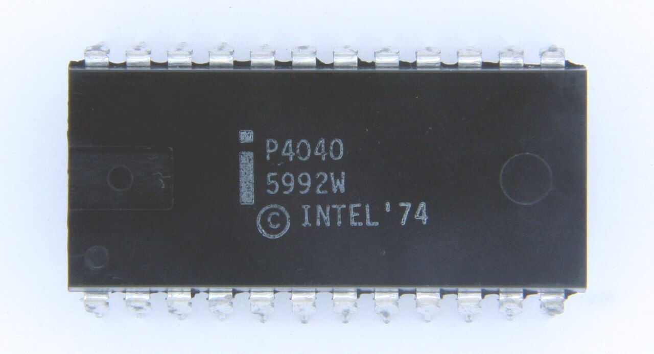
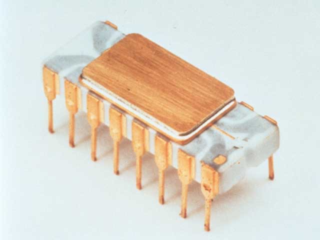
The Intel 4040 is a 4-bit microprocessor introduced in 1974 as the successor to the Intel 4004. It was the second 4-bit microprocessor designed and manufactured by Intel, produced with a 10 μm process using silicon gate enhancement-load PMOS logic technology. The 4040 contained 3,000 transistors and could execute approximately 62,000 instructions per second. Its main improvements over the 4004 included a larger 24-pin package, support for interrupts, a halt/stop system for low-power and single-step debugging, and expanded ROM addressing via bank selection.
Quick Facts
- Produced-Start
- 1974
- Produced-End
- 1981
- Slowest
- 500
- Slow-Unit
- kHz
- Fastest
- 740
- Data-Width
- 4 bits
- Address-Width
- 12 bits (multiplexed)
- Arch
- 4-bit (BCD-oriented)
- Transistors
- 3,000
- Predecessor
- Intel 4004
- Support Status
- Unsupported
Facts from the source article.
Lore & Background
The 4040 was essentially an expansion of the 4004, with additional pins, more registers, and new instructions. The 4004 had a single ROM pin, whereas the 4040 added another ROM pin to allow two banks of ROM, effectively increasing the ROM address from 12 to 13 bits (8 KB). Unlike later designs where two lines could be binary encoded to support four banks, the ROM chips used with the 4004 and 4040 used these lines like chip select pins, supporting only two banks. The 4004 lacked interrupts, a serious limitation for real-time applications; the 4040 added a new input pin for calling an interrupt and an output pin to acknowledge it. The stack register file was expanded to seven entries, up from three. To speed interrupt handling, eight additional registers were added in a new 'bank 1', with the original sixteen registers becoming 'bank 0'. When an interrupt was received, a single instruction could swap banks, allowing the handler to use the first eight registers without disturbing the original values. Another addition was the input stop pin and associated output stop acknowledge, which could stop the processor for I/O or debugging, putting most chip hardware into a low-drain, high-impedance condition while keeping machine cycle clocks running for external devices. The instruction set was expanded to 60 instructions from the original 46, adding support for logical AND and OR operators.
Reader's Guide
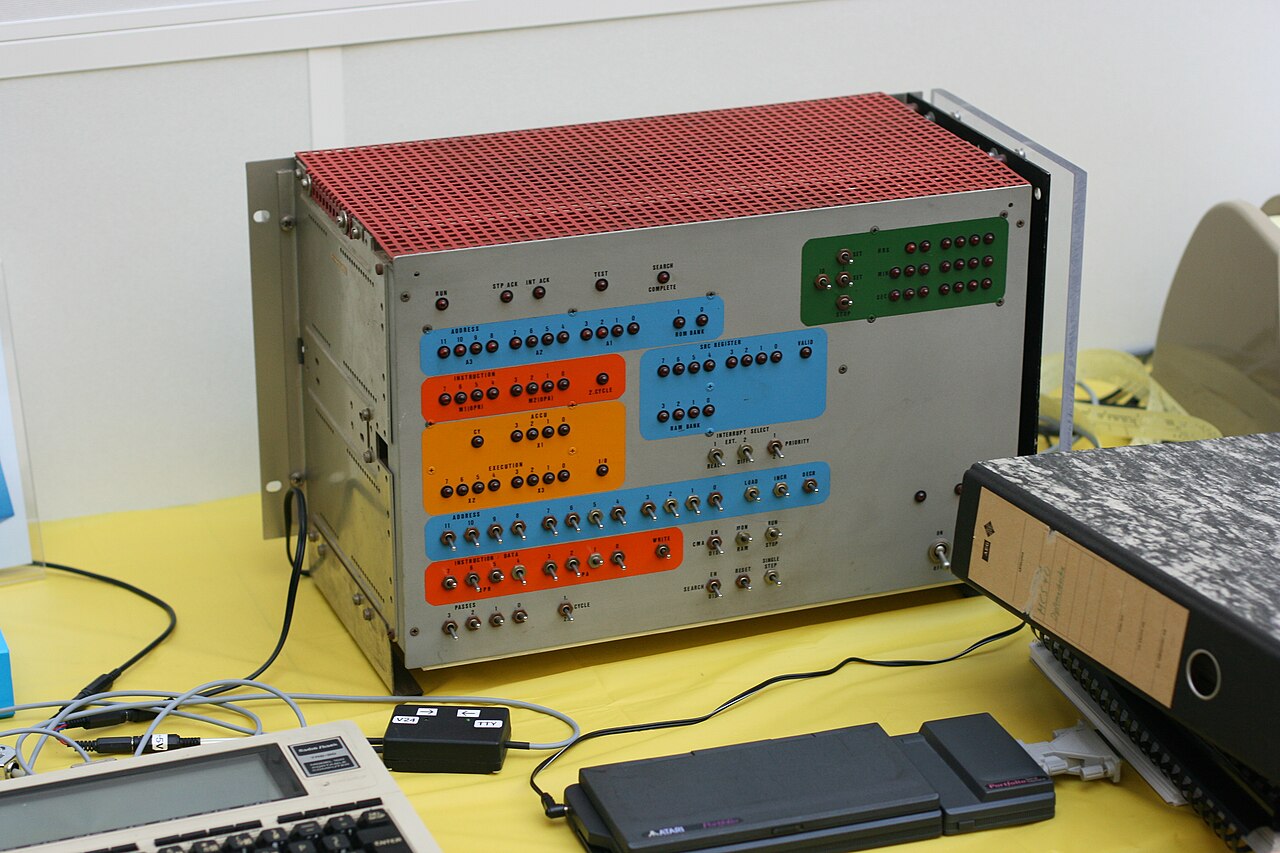
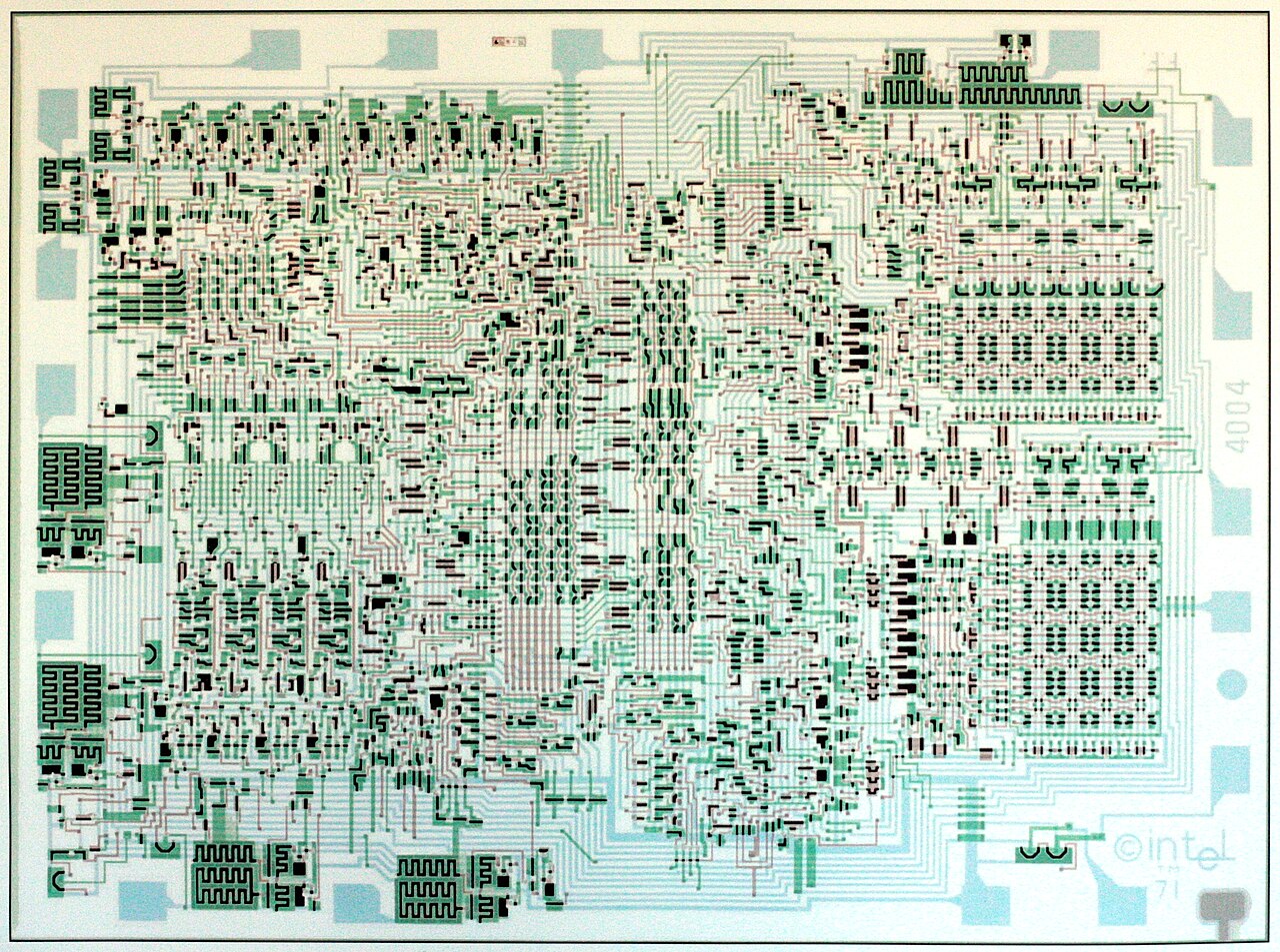
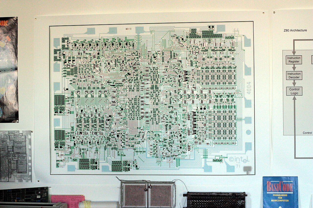
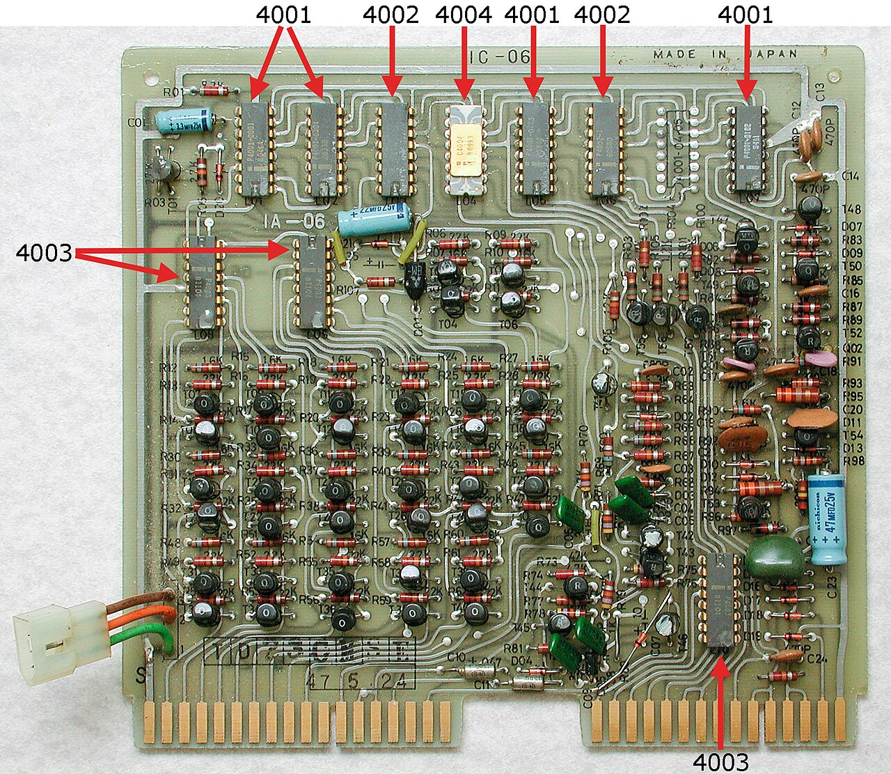
The Intel 4040 addressed several limitations of the 4004, most notably the lack of interrupts, which had been considered a major oversight. By adding interrupt support, a halt/stop system, and bank-switched ROM, the 4040 became more suitable for real-time and debugging applications. The expanded register file and bank-switching mechanism allowed rapid interrupt response with minimal overhead. The 4040 was first used in a microcomputer in Intel's Intellec 4 Mod 40 development system, released in early 1975. According to Byte magazine, the first third-party microcomputer designed around the Intel 4040 was the Micro 440, released by Comp-Sultants of Huntsville, Alabama, in late 1975. A range of new support chips were introduced for the 4040, including RAM, ROM, EPROM, clock generators, I/O ports, a programmable keyboard/display controller, and a standard memory interface. The 4040's design was proposed by Federico Faggin, who formulated the architecture and led the design; detailed design was done by Tom Innes. The original mask shows Tom Innes' initials (TI) alongside two further initials from sofar unidentified other designers (JO, EL).
Did You Know?
- The 4040 was produced with a 10 μm process and contained 3,000 transistors.
- It added interrupts, which the 4004 lacked and which were considered a major oversight.
The 16-Bit Foundations: From Stopgap to Standard
Intel's microarchitecture story begins not with a grand vision but with a pragmatic stopgap. The 8086, the very first x86 processor, was conceived as a temporary bridge while the more ambitious iAPX 432 was still in development. Its real mission was competitive: to outmaneuver Motorola, Zilog, and National Semiconductor, and to surpass the already-successful Z80 in the microprocessor market. The 8088 variant, featuring an 8-bit external bus, found its most iconic home inside the original IBM Personal Computer, cementing the x86 lineage in the personal computing world. The 186 generation moved toward integration, embedding a DMA controller, interrupt controller, timers, and chip-select logic onto the die, while the 80188 offered an 8-bit bus option. The 286 marked a genuine architectural leap: it was the first x86 chip to implement protected mode with segmentation-based virtual memory management, delivered a 24-bit address bus, and delivered roughly three to four times the performance of the 8086. These early chips laid the structural vocabulary that every subsequent generation would build upon.
The 32-Bit Leap and the Birth of Modern Execution
The transition to 32-bit computing reshaped what a microprocessor could do. The i386 introduced paging layered atop segmentation, a memory-protection mechanism that remains the backbone of virtually every modern operating system. The i486 followed with a built-in floating-point unit, 8 KB of on-chip L1 cache, and pipelining, making each megahertz measurably more productive than its 386 predecessor. The P5 generation, known as the original Pentium, broke new ground by becoming the first x86 processor with a super-scalar design and hardware branch prediction. The P6 family, spanning Pentium Pro through Pentium III Xeon, pushed further still: it was the first x86 to support SIMD instructions via XMM registers, adopted a RISC-style micro-op decode scheme, integrated register renaming with out-of-order execution, and introduced conditional move instructions to sidestep costly branch penalties. It also added 36-bit physical address extension, a capability that would prove essential as memory capacities grew.
The 64-Bit Era and the AVX Revolution
Once Intel crossed into 64-bit territory, the pace of architectural innovation accelerated. The Core microarchitecture, built on a 65 nm process, reengineered the P6 design with a wider front end, enhanced macro-op and micro-op fusion, a larger out-of-order core, and a bigger renamed register file. Nehalem, released in November 2008 on 45 nm, made a structural shift by integrating the memory controller directly onto the CPU die and adding SSE4.2 instructions. Sandy Bridge, arriving in January 2011 at 32 nm, delivered the first 256-bit AVX instruction set and the YMM registers, a milestone for parallel computing workloads. Haswell, in June 2013 at 22 nm, extended the vector toolkit with AVX2 and FMA. By the time Skylake-X hit high-end desktop and server markets in 2017, the architecture supported the full AVX-512 instruction set, pushing the width of parallel data processing to new heights and setting the stage for AI and scientific computing workloads.
Tick-Tock, Naming Schemes, and Strategic Shifts
For decades Intel's roadmap followed a predictable rhythm: the tick-tock model alternated between process-node shrinks (ticks) and new microarchitectures (tocks), later refined into a process-architecture-optimization cadence. That rhythm finally broke with Kaby Lake in August 2016, when delays in the 10 nm process forced Intel to hold at 14 nm. A string of 14++ nm successors followed—Coffee Lake, Comet Lake, and the AI-optimized Cooper Lake—each stretching the same node further. The naming conventions also evolved. Starting with Cannon Lake, Intel decoupled core codenames from product codenames, a change visible in the Palm Cove core that shipped in only one chip before the project was cancelled. Cannon Lake itself, the first and only microarchitecture to implement Palm Cove, launched in May 2018 on 10 nm and was discontinued by December 2019. Sunny Cove, its intended successor, became the first non-Atom core to include hardware acceleration for SHA hashing, signaling a continued push toward specialized on-die functionality even as the broader roadmap grew more complex.
Gallery
Frequently Asked Questions
What is the Intel 4040?
The Intel 4040 is a 4-bit microprocessor that Intel released in 1974 as the direct successor to the original 4004. It represents Intel's second foray into 4-bit microprocessor design and was built using a 10 μm silicon-gate PMOS process.
How did the Intel 4040 improve on the Intel 4004?
It introduced hardware interrupt support, a halt/stop mechanism for low-power standby and single-step debugging, and bank-switched ROM addressing that effectively extended the address space beyond the base 12-bit limit. The chip also moved to a larger 24-pin package to accommodate the added functionality.
What are the key specifications of the Intel 4040?
The 4040 contains roughly 3,000 transistors, executes about 62,000 instructions per second, and features a 4-bit data bus with a 12-bit ROM address bus (effectively 13 bits when bank switching is used). It was fabricated with a 10 μm enhancement-load PMOS logic process.
What logic technology did the Intel 4040 use?
It employed silicon-gate enhancement-load PMOS logic at a 10 μm process node, a step in manufacturing refinement over earlier Intel 4-bit designs. This technology kept the chip in the PMOS family rather than jumping to the CMOS or NMOS approaches that would dominate later.
Why does the Intel 4040 matter in microprocessor history?
It marked the point where Intel moved beyond the bare-bones 4004 toward chips with practical system-level features like interrupts and debug halts, making 4-bit processors genuinely usable in embedded control applications. As the bridge between the 4004 and the 8-bit era, it helped establish the architectural patterns that carried forward into the 8080 and beyond.
More in Intel and AMD Microprocessors 1-24
Spotted an error? Know more?
Reader corrections go straight into our review queue. Suggest an edit · How this site is sourced