Intel 8008
An early 8-bit microprocessor that powered the first personal computers.

Appaloosa · CC BY-SA 3.0
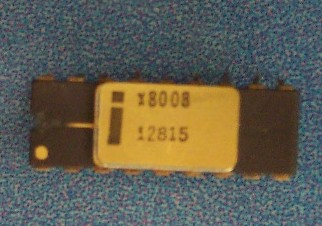
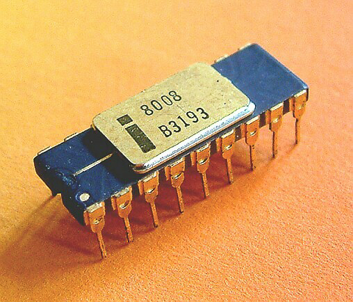
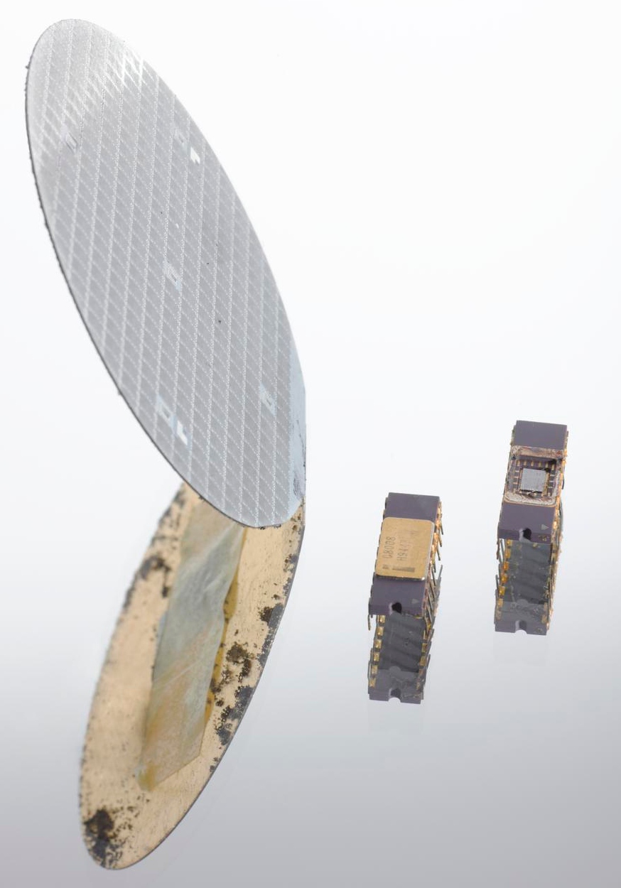
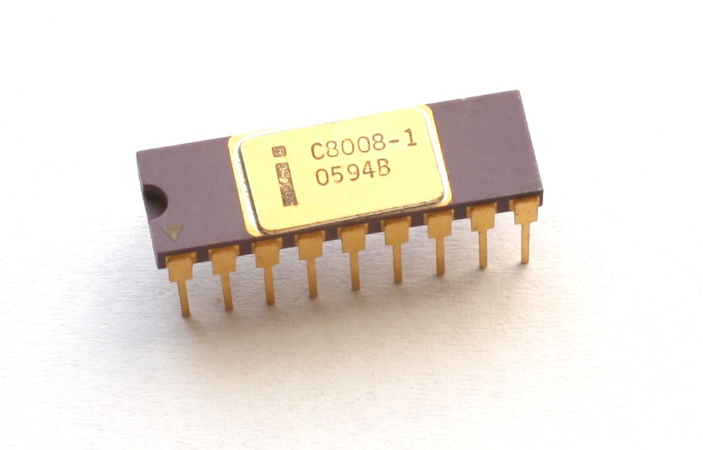
The Intel 8008 is an early 8-bit microprocessor introduced in April 1972. It is notable as the CPU used in the first commercial non-calculator personal computers and as a precursor to the Intel 8080 and the x86 family.
Quick Facts
- Produced-Start
- April 1972
- Produced-End
- 1983
- Slowest
- 500
- Slow-Unit
- kHz
- Fastest
- 800
- Transistors
- 3,500
- Application
- Computer terminals, calculators, bottling machines, 1970s ASEA industrial robots (IRB 6), simple computers, etc.
- Designfirm
- Computer Terminal Corporation (CTC)
- Arch
- 8008
- Successor
- Intel 8080
- Data-Width
- 8 bits
Facts from the source article.
Lore & Background
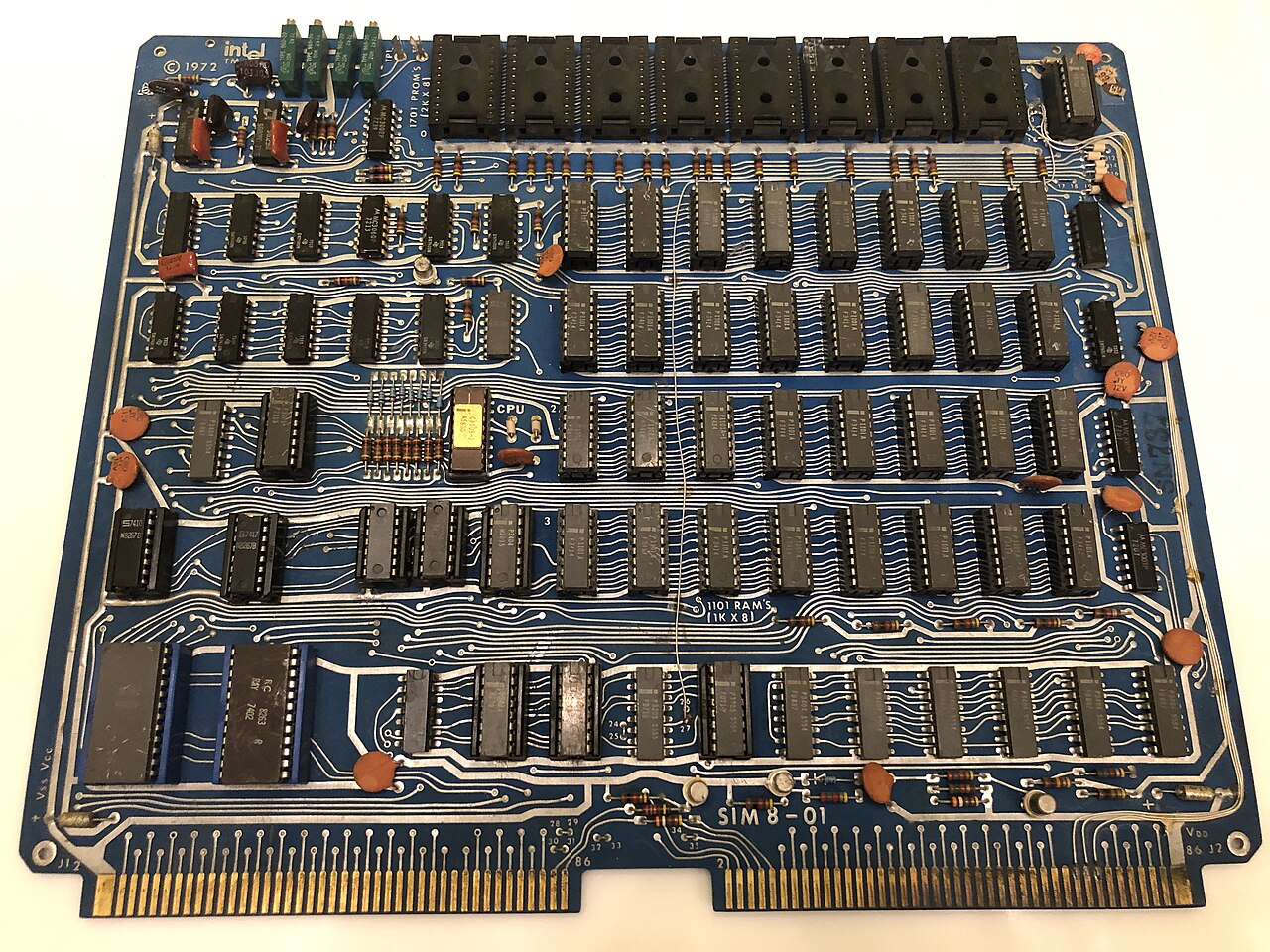
The 8008 architecture was designed by Computer Terminal Corporation (CTC) and implemented by Intel. Originally intended for CTC's Datapoint 2200 programmable terminal, the chip was developed after CTC sought a single-chip CPU to replace a custom logic chipset. Intel engineer Stan Mazor proposed a one-chip programmable microprocessor, and development began under the name 1201. Texas Instruments also produced samples as the TMX 1795, but these were buggy and rejected. CTC later released the Datapoint 2200 using discrete TTL logic, pausing the 1201 project. In early 1971, Seiko expressed interest in using the 1201 for a scientific calculator, leading to a redesign under Federico Faggin that expanded the chip from 16 to 18 pins. The 1201 was delivered to CTC in late 1971, but CTC had moved on to a faster parallel-architecture terminal and ended involvement, leaving the intellectual property to Intel. Intel renamed it the 8008 and cataloged it in April 1972 at US$120. The 8008 was used in the SCELBI kit, the Micral N, and the MCM/70 personal computers, as well as in Hewlett-Packard's 2640 terminal family. In 1973, Intel offered an instruction set simulator for the 8008 named INTERP/8, written in FORTRAN IV by Gary Kildall.
Reader's Guide
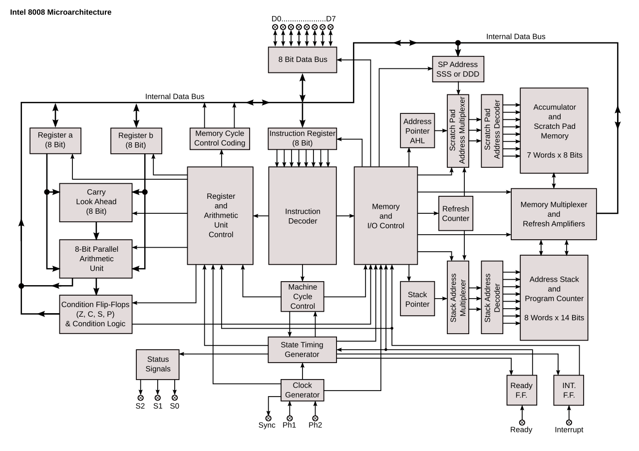
The Intel 8008 holds significance as the CPU for the first commercial non-calculator personal computers, including the US SCELBI kit, the French Micral N, and the Canadian MCM/70. It also served as the controlling microprocessor for early Hewlett-Packard 2640 terminals. Although slower in instructions per second than the 4-bit Intel 4004, the 8008 processed data 8 bits at a time and accessed more RAM, giving it a speed advantage in most applications. Its architecture, with 48 instructions, a 14-bit program counter, and a seven-level call stack, directly influenced the subsequent Intel 8080, which expanded upon its registers and instruction set. The 8080 was not binary compatible with the 8008, but assembler-language code for the 8008 could be assembled into 8080 machine code. The Intel 8086, the original x86 processor, is a non-strict extension of the 8080, meaning almost every 8008 instruction has an equivalent in modern x86 processors, though encodings differ. The 8008's design, limited by its 18-pin package, required about 30 TTL support chips to interface with memory, reflecting the constraints of early microprocessor integration.
Did You Know?
- The 8008 was originally named the 1201 during development.
- Seiko's interest in using the 1201 for a scientific calculator prompted a redesign that expanded the chip from 16 to 18 pins.
- The 8008 can access 8 input ports and 24 output ports.
- Gary Kildall wrote the INTERP/8 instruction set simulator for the 8008 in FORTRAN IV.
The Chiplet Revolution: From Monolithic Silicon to Disaggregated Modules
One of the most consequential structural shifts in Intel's modern roadmap is the transition from single-die processors to multi-chip module designs. Meteor Lake, launched in December 2023 as Core Series 1, marked the first time Intel deployed a chiplet architecture in a mobile generation, assembling the processor from multiple distinct dies on a shared package. Its successor, Arrow Lake (Core Series 2, released October 24, 2024), extended this disaggregated MCM approach to desktop platforms for the first time, broadening the design philosophy beyond the mobile-only constraint that had limited Meteor Lake. A notable architectural consequence of this new generation is the elimination of Hyper-Threading across both Arrow Lake and Lunar Lake parts, signaling a departure from a technique that had defined Intel's performance strategy for over a decade. The value tier within Core Series 2 further illustrates the complexity of this transition, as some low-power mobile parts are actually re-refreshed Raptor Lake silicon rather than true Arrow Lake variants, blurring the line between generations within a single product family.
The Branding Overhaul: Ditching the i3/i5/i7/i9 Legacy
In June 2023, Intel executed a significant rebranding of its consumer and commercial processor lines, retiring the long-standing Core i3, i5, i7, and i9 nomenclature that had anchored the company's marketing for roughly a decade. The new system splits the lineup into two distinct brands: Core, positioned for everyday and value-oriented computing, and Core Ultra, reserved for premium-tier processors. Each brand is further subdivided into numeric tiers—Core 3, 5, 7, 9 and Core Ultra 3, 5, 7, 9—creating a clearer hierarchy that separates budget and mainstream offerings from high-end performance parts. This restructuring was rolled out alongside the Meteor Lake launch and has since propagated through subsequent generations. Core Series 1 (December 2023), Core Series 2 (October 2024), Core Series 2 Plus (March 2026, an Arrow Lake refresh), and Core Series 3 (announced at CES 2026, January 5, 2026, codenamed Panther Lake) all inherit this dual-brand framework, establishing a consistent naming architecture that Intel intends to carry forward across its evolving product portfolio.
Power Tiers, Form Factors, and the Handheld Gaming Frontier
Intel's modern product segmentation has grown remarkably granular, carving the mobile and embedded space into multiple power and performance bands. Within the premium mobile tier, processors are categorized by High Power, Low Power, and Ultra Low Power envelopes, each with distinct thermal and performance targets. The Ultra Low Power segment, exemplified by Lunar Lake-based parts, integrates on-package LPDDR5X-8533 memory directly onto the package, eliminating the need for discrete RAM modules. For thin-and-light laptops, certain high-power mobile parts are soldered onto the motherboard using the BGA1792 socket, locking the processor in place for space-constrained designs. The value tier fills the budget segment with re-refreshed Raptor Lake and Alder Lake E-Core-only parts. Perhaps most strikingly, the Panther Lake generation (Core Series 3) introduces dedicated handheld gaming processors alongside mobile parts, while Xeon 6+ targets network infrastructure and data center servers with support for up to 1.5 TB of DDR5 RDIMM 8000MT/s RAM, demonstrating how Intel's segmentation now spans from pocket-sized gaming devices to enterprise racks.
Platform Features, Sockets, and the Enterprise Feature Stack
The underlying platform infrastructure accompanying each Intel generation carries substantial weight in enterprise and workstation adoption. Socket designations have shifted from LGA 1700 (used by 12th, 13th, and 14th generation desktop parts) to LGA 1851 for Arrow Lake and its refresh, reflecting physical and electrical changes in the platform. Enterprise features are layered through chipset-specific support: the W680 chipset enables UDIMM ECC memory on 12th through 14th generation desktop parts, while the W880 chipset extends ECC support to Arrow Lake desktop processors. Intel vPRO, the company's manageability and security suite, appears in both Enterprise and entry-level workstation flavors, with underlined models in product tables indicating which SKUs carry the feature. The Core Series 3 Panther Lake generation restricts itself to mobile and handheld gaming parts, while Core Series 2 Plus (Arrow Lake Refresh, March 26, 2026) continues on LGA 1851. Certain value-tier models participate in Intel's SIPP (Stable IT Platform Program), offering longer support windows for IT fleet deployments, and Xeon 6+ parts support Intel Speed Select for workload-tuned frequency management in data center environments.
Gallery
Frequently Asked Questions
What is the Intel 8008?
The Intel 8008 is an 8-bit microprocessor that Intel released in April 1972. It is best remembered as the chip that went inside the first commercial personal computers that weren't just calculators.
What are the key specs of the Intel 8008?
It contains 3,500 transistors, runs at up to 0.8 MHz in its 8008-1 variant, and can address a maximum of 16 KB of memory. The chip ships in an 18-pin dual in-line package.
What was the Intel 8008 actually used in?
It served as the central processor in the earliest non-calculator personal computers, giving hobbyists and small businesses a way to build programmable machines on a desk rather than in a data center.
How does the Intel 8008 connect to the x86 family?
The 8008 is a direct architectural ancestor of the Intel 8080, which in turn laid the groundwork for the 8086 and the entire x86 instruction-set lineage that still dominates computing today.
Why do microprocessor fans still care about the Intel 8008?
It marks the moment a single chip could run a full general-purpose program outside of a mainframe, making it a foundational milestone in the history of personal computing.
More in Intel and AMD Microprocessors 1-24
Spotted an error? Know more?
Reader corrections go straight into our review queue. Suggest an edit · How this site is sourced