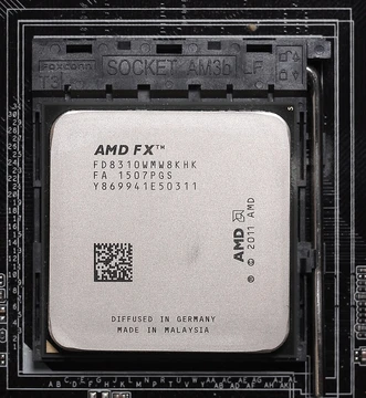
Intel 8080
Intel's 8-bit microprocessor that spurred the microcomputer revolution.

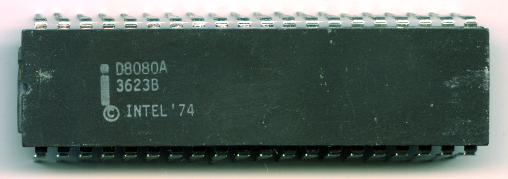
AntonSor at Russian Wikipedia · Public domain
The Intel 8080, an 8-bit microprocessor from Intel, hit the market in April 1974 as the follow-up to the 8008, though programs written for the older chip wouldn't run on it directly. It was initially aimed at embedded roles—think calculators, cash registers, computer terminals, and industrial robots—but its popularity exploded, helping to kickstart the microcomputer era.
Several design decisions fueled its success. A 40-pin package made connecting it to other parts much easier than the 8008's cramped 18-pin layout, giving it a more efficient data bus. Switching from PMOS to NMOS technology boosted transistor speed and made the chip compatible with TTL logic. An expanded instruction set and a full 16-bit address bus let the 8080 address up to 64 KB of memory—four times what the 8008 could handle. A wider array of support chips also extended its capabilities. Many of these improvements came directly from customer complaints about the 8008's shortcomings, which designer Federico Faggin and others at Intel heard on the road.
The 8080 powered early personal computers like the Altair 8800 and other S-100 bus machines, and it was the original target for the CP/M operating system. It also left a lasting mark on computing: the later x86 architecture was deliberately designed so its assembly language closely mirrored the 8080's, allowing many instructions to map straight across.
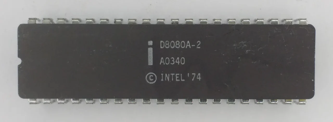
The base model ran at 2 MHz, with common instructions taking 4 to 11 clock cycles, managing several hundred thousand instructions per second. Faster variants arrived later: the 8080A-1 hit 3.125 MHz, and the 8080A-2 ran at 2.63 MHz. In most setups, the processor worked alongside two support chips: the 8224 clock generator/driver and the 8228 bus controller, which handled timing and data flow.
**History**
Customers had been slow to adopt the 8008 due to its single addressing mode, low clock speed, limited pin count, and small on-chip stack, which cramped software complexity. Several designs for the 8080 were floated, from simply tacking stack instructions onto the 8008 to a complete break from Intel's earlier architectures. The final design was a middle ground.
Work on the 8080 began in the summer of 1971, right after Intel finished the 4004 and while the 8008 was still in development. As word about "CPU on a chip" spread, Intel saw interest from all kinds of customers.
Quick Facts
- Slowest
- 2
- Slow-Unit
- MHz
- Fastest
- 3.125
- Soldby
- Intel
- Arch
- 8080
- Transistors
- 4,500 or 6,000
- Data-Width
- 8 bits
- Address-Width
- 16 bits
- Numcores
- 1
- Predecessor
- Intel 8008
- Successor
- Intel 8085
Facts from the source article.
Lore & Background
The conception of the 8080 began in the summer of 1971, when Intel wrapped up development of the 4004 and were still working on the 8008. After rumors about the 'CPU on a chip' came out, Intel started to see interest in the microprocessor from all sorts of customers. Federico Faggin, who led the design of the 4004 and became the primary architect of the 8080, found that customers were complaining about the architecture and performance of the 8008, as its speed at 0.5 MHz was 'not adequate.' Faggin later proposed the chip to Intel's management and pushed for its implementation in the spring of 1972, but Intel did not approve the project until fall of that year. Faggin hired Masatoshi Shima from Japan in November 1972 to do the detailed design under his direction. Shima finished the layout in August 1973, and production began in December of that year. A prototype was completed in January 1974, and after working out last-minute issues, Intel introduced the product in March 1974, releasing it a month later as requiring Low-power Schottky TTL devices. The 8080A fixed a flaw related to ground voltage when driving with standard TTL devices.
Reader's Guide
The Intel 8080 is notable for several key design choices that contributed to its success. Its 40-pin package simplified interfacing compared to the 8008's 18-pin design, enabling a more efficient data bus. The transition to NMOS technology provided faster transistor speeds than the 8008's PMOS, also making it TTL compatible. An expanded instruction set and a full 16-bit address bus allowed the 8080 to access up to 64 KB of memory, quadrupling the capacity of its predecessor. Many of these improvements stemmed from customer feedback. The 8080 found its way into early personal computers such as the Altair 8800 and subsequent S-100 bus systems, and it served as the original target CPU for the CP/M operating system. It directly influenced the later x86 architecture, which was designed so that its assembly language closely resembled that of the 8080, permitting many instructions to map directly from one to the other. The 8080 was explicitly designed to be a general-purpose microprocessor for a larger number of customers, and much of the development effort was spent trying to integrate the functionalities of the 8008's supplemental chips into one package.
Did You Know?
- The 8080 was not binary compatible with its predecessor, the 8008, but was source compatible once run through a transpiler.
- Intel offered an instruction set simulator for the 8080 named INTERP/80, written in FORTRAN IV by Gary Kildall.
- The 8080's stack was moved to external memory to expand the capabilities of stack-based routines and interrupts.
- There is only one patent on the 8080, listing Federico Faggin, Masatoshi Shima, and Stanley Mazor.
Architectural Vision and the Deliberate Break with the 8008
The 8080 was born from a conscious decision to stop treating the 8008 as a ceiling. Rather than simply bolting new instructions onto the older chip, the Intel team chose a middle path between incremental tweaks and a total architectural overhaul. Federico Faggin, who had led the 4004 design, became the primary architect after hearing directly from customers that the 8008's 0.5 MHz speed and single addressing mode were simply not adequate for real-world work. The final design incorporated a 40-pin package that simplified board interfacing compared to the 8008's 18-pin layout, a shift to NMOS fabrication for faster transistor switching and TTL compatibility, and a full 16-bit address bus that quadrupled accessible memory to 64 KB. The team also made the deliberate choice to forgo binary compatibility with the 8008, instead targeting source-level compatibility through a transpiler. That freedom let them move the stack into external memory, expand interrupt handling, and assign specialized roles to register pairs—choices that freed transistors for other functions and gave programmers far more expressive power than the 8008's limited model allowed.
From Management Rejection to a Flawed Prototype
The path to the 8080 was neither smooth nor swift. Conception began in the summer of 1971, as Intel was wrapping up the 4004 and still working through the 8008. Faggin, while giving technical seminars and visiting customers, collected complaints about the existing architecture's shortcomings. He proposed the new chip to Intel management in spring 1972, only to be met with surprise and frustration when the project was denied. Intel wanted to gauge market reaction to its existing products and was preoccupied with shipping its latest memory chips. Approval finally came in the fall of 1972. Faggin then recruited Masatoshi Shima from Japan in November of that year; Shima had previously helped design the 4004's logic and would handle the detailed design under Faggin's direction, applying the random-logic silicon-gate methodology Faggin had developed. Shima completed the layout in August 1973, and production began in December. A prototype was finished in January 1974, but it carried a flaw: driving it with standard TTL devices pushed up ground voltage due to high current on a narrow line. Intel had already produced 40,000 units at the sales department's urging before Shima characterized the prototype. After resolving last-minute issues, the product was introduced in March 1974 and formally released in April, specifying Low-power Schottky TTL devices. The 8080A variant later corrected the grounding flaw.
Sparking the Microcomputer Revolution
The 8080's influence on the trajectory of personal computing is difficult to overstate. Originally conceived for embedded applications—calculators, cash registers, computer terminals, industrial robots—it far outgrew that niche. The processor became the central brain of the Altair 8800 and the broader S-100 bus ecosystem that followed, giving hobbyists and early entrepreneurs a practical platform for building their own machines. Gary Kildall, working as a consultant for Intel, wrote an instruction set simulator called INTERP/80 in FORTRAN IV to run compiled PL/M programs, and the 8080 went on to serve as the original target CPU for the CP/M operating system. Perhaps most enduringly, the 8080's design philosophy directly shaped the x86 architecture that would dominate computing for decades. The x86 was deliberately constructed so that its assembly language closely mirrored the 8080's, allowing many instructions to map directly between the two. This lineage means that the architectural decisions Faggin, Shima, and Stanley Mazor made in the early 1970s—specialized registers, the instruction set structure, the programming model—echo through virtually every x86 processor to this day. The single patent covering the 8080 lists all three names.
Performance Profile and the Supporting Chip Ecosystem
In its original form, the 8080 operated at a 2 MHz clock rate, with common instructions requiring between 4 and 11 clock cycles to complete. This translated to a throughput of several hundred thousand instructions per second—a significant leap over the 8008's 0.5 MHz. Intel later introduced two faster variants: the 8080A-2 at 2.63 MHz and the 8080A-1 at 3.125 MHz, giving system designers more headroom for demanding applications. In typical deployments, the processor was not used in isolation. It was paired with two dedicated support chips: the 8224, which handled clock generation and driving, and the 8228, a bus controller that managed data flow across the system. A broader selection of support chips further extended the 8080's capabilities beyond what the 8008 ecosystem offered. The shift to NMOS technology was central to the performance gains, delivering faster transistor switching than the 8008's PMOS construction while also making the chip directly compatible with TTL logic families. The expanded instruction set, which added 16-bit operations and direct addressing modes for the full 64 KB memory space, gave programmers far more flexibility than the 8008's reliance on the HL register pair for indirect access to its 14-bit address space.
Gallery
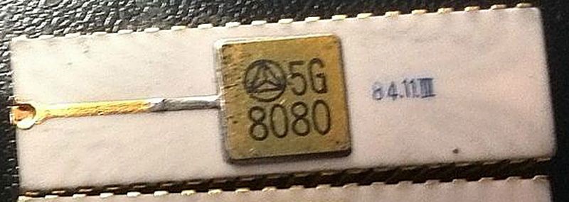
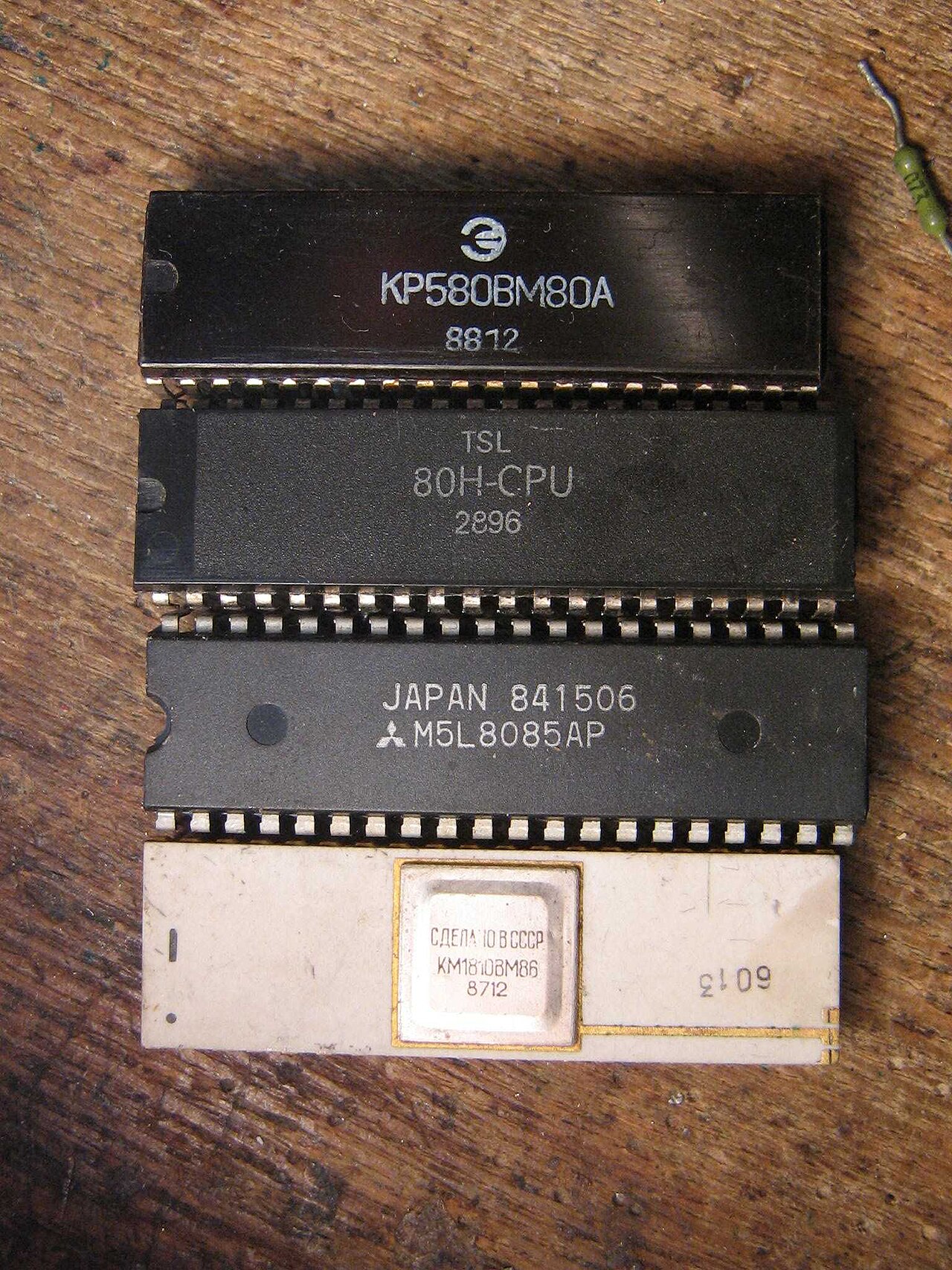
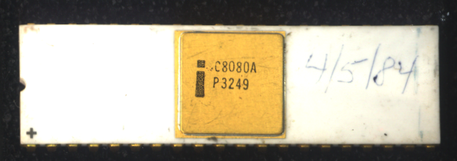
Frequently Asked Questions
What is the Intel 8080?
The Intel 8080 is an 8-bit microprocessor that hit the market in April 1974 as the successor to Intel's 8008. It came in a 40-pin DIP package, ran at a 2 MHz clock speed, and could address up to 64 KB of memory through its 16-bit address bus.
How did the 8080 differ from the 8008 it replaced?
Despite being the 8008's follow-up, the two chips were not instruction-set compatible, so code written for one would not run on the other. The 8080 also switched from PMOS to NMOS technology and replaced the 8008's cramped 18-pin layout with a far more practical 40-pin package.
Why is the Intel 8080 considered so important?
Although Intel initially aimed it at embedded applications like calculators, cash registers, and industrial robots, the 8080's ease of integration and solid performance made it a favorite among hobbyists and early system builders. That broad appeal helped ignite the microcomputer revolution of the mid-1970s.
What were the 8080's core specifications?
The original 8080 clocked at 2 MHz, while the 8080A-1 variant pushed to 3.125 MHz and the 8080A-2 to 2.63 MHz. It featured an 8-bit data path, a 16-bit address bus supporting 64 KB of addressable memory, and shipped in a 40-pin DIP.
What kinds of devices actually used the Intel 8080?
Intel originally marketed the chip for embedded roles such as computer terminals, cash registers, calculators, and industrial control robots. Its popularity eventually spread into early personal computers, cementing its place as the processor that helped launch the home-computing era.
More in Intel and AMD Microprocessors 1-24
Spotted an error? Know more?
Reader corrections go straight into our review queue. Suggest an edit · How this site is sourced