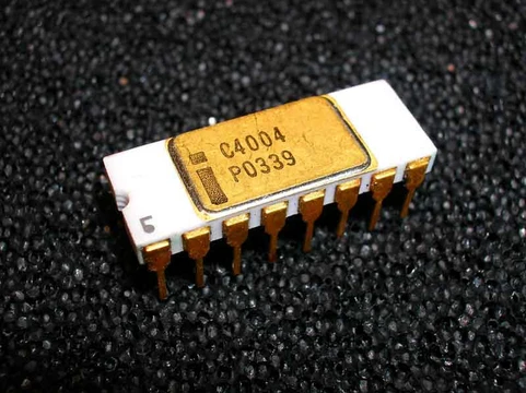
TRIPS architecture
EDGE-based processor using compiler-scheduled hyper-blocks for high parallelism.

fotokoci · CC0
TRIPS (Tera-op, Reliable, Intelligently adaptive Processing System) is a microprocessor architecture based on the Explicit Data Graph Execution (EDGE) concept, developed by a team at the University of Texas at Austin in conjunction with IBM, Intel, and Sun Microsystems. It is notable for its attempt to bypass performance bottlenecks in traditional processors by using compiler-constructed hyper-blocks of instructions that are distributed to independent processing elements, aiming to achieve high parallelism and reduce data movement overhead.
- Developer
- University of Texas at Austin, IBM, Intel, Sun Microsystems
- Architecture
- EDGE (Explicit Data Graph Execution)
- Prototype cores per chip
- 2
- Functional units per core
- 16
- Arrangement
- 4-wide, 4-deep
- Hyper-block size
- 128 instructions
- Blocks in flight per core
- 8
Lore & Background
The TRIPS architecture was designed as an implementation of the EDGE concept, which reimagines how a processor interprets instruction streams. Instead of treating instructions as a linear sequence, EDGE compilers analyze code to find blocks of instructions that share data dependencies, assembling them into compiled 'hyper-blocks.' These hyper-blocks are fed into the CPU along with the data they need, allowing the processor to isolate each block in a single functional unit with its own local memory. This approach reduces expensive memory reads and writes by keeping data in high-speed memory close to the processing elements.
The prototype TRIPS processor contains two complete cores, each with 16 functional units arranged in a four-wide, four-deep configuration. The compiler constructs hyper-blocks of 128 instructions each, and the system can keep eight blocks 'in flight' per core, totaling 1,024 instructions per core. The design is built by repeating a single basic functional unit, which is general-purpose and can run any instruction type. This avoids the need to balance different kinds of cores and allows the processor to scale performance linearly with the number of cores.
TRIPS aimed to reach 1 TFLOP on a single processor, as described in papers published from 2003 to 2006. The basic design can include up to 32 chips interconnected, approaching 500 GFLOPS. The architecture's reliance on compiler capabilities for parallelism, rather than on-chip scheduling, allows it to scale wider and deeper than traditional designs, which typically plateau at four-wide parallelism.
Reader's Guide
The TRIPS architecture represents a significant departure from conventional processor design by shifting the burden of instruction scheduling from hardware to the compiler. Its EDGE foundation allows the processor to examine thousands of instructions at once—hundreds per hyper-block and hundreds of hyper-blocks—leading to greatly improved functional unit utilization. Compared to a typical four-issue superscalar design, TRIPS can process about three times as many instructions per cycle.
A key advantage of TRIPS is its 'polymorphic' nature: because every functional unit is general-purpose, the processor maintains consistent performance across diverse workloads. In traditional CPUs, a math-heavy workload bogs when floating-point units are busy while integer units idle, and a data-intensive workload does the opposite. TRIPS avoids this imbalance, as every unit contributes to every task. This makes it potentially competitive with specialized processors like DSPs for certain workloads, while retaining the ability to run general-purpose code.
The architecture also reduces global register file size, which has become a bottleneck in modern processors as chip sizes shrink but distances to registers grow. By keeping data local to functional units or in well-defined inter-core links, TRIPS eliminates long cross-chip delays, allowing individual cores to run at higher speeds. However, by 2008, GPUs from ATI and NVIDIA had already exceeded 1 teraflop for specialized applications, while a contemporary 2007 Mac Pro with a 2-core Intel Xeon achieved only about 5 GFLOPs on single applications. TRIPS thus offered a path toward high-performance general-purpose computing, though its full potential remained unrealized in commercial hardware.
Did You Know?
- TRIPS stands for Tera-op, Reliable, Intelligently adaptive Processing System.
- The prototype chip has two complete cores, each with 16 functional units in a 4-wide, 4-deep arrangement.
- The compiler constructs hyper-blocks of 128 instructions, and the system keeps eight blocks in flight per core.
Origins & Collaborative Vision
TRIPS — standing for Tera-op, Reliable, Intelligently adaptive Processing System — emerged from a partnership between the University of Texas at Austin and three industry giants: IBM, Intel, and Sun Microsystems. The project's ambition was bold: the research team, publishing papers between 2003 and 2006, set a target of one teraflop of performance from a single processor. Their prototype chip embodied this vision with sixteen independent processing elements, each capable of executing its own stream of work without waiting on the others. The collaboration blended academic research freedom with the engineering muscle of major hardware companies, giving the team both the theoretical latitude to rethink processor design from the ground up and the practical resources to build a working silicon implementation. Rather than incrementally improving the superscalar designs that dominated the early 2000s, the TRIPS team chose to question the fundamental assumptions about how instructions flow through a chip and how data moves between functional units.
The EDGE Philosophy
At the heart of TRIPS lies the Explicit Data Graph Execution concept, which reframes the processor's relationship with the instruction stream. Instead of viewing code as a linear sequence of individual operations, EDGE treats it as a collection of related instruction blocks — called hyper-blocks — that share data in specific, compiler-verified ways. The compiler's job is to scan the program, identify where values flow from one operation to another, and package those operations together with all the data they require into a single self-contained unit. A simple example illustrates the shift: a program that reads two numbers from memory, adds them, then adds the result to a third memory value would, on a conventional CPU, require careful scheduling and intermediate register storage. Under EDGE, the compiler bundles all three operations and their operands into one hyper-block, delivered to a single functional unit with its own private registers. No extra memory fetches are needed, and the data never has to travel far. When data must be handed off between blocks, the compiler explicitly encodes that transfer so the hardware can schedule it in the correct order, spreading communications to prevent transport bottlenecks.
Polymorphic Processing
One of TRIPS's most distinctive design choices is the elimination of specialized functional units. Traditional superscalar processors dedicate separate hardware for integer arithmetic, floating-point math, and memory operations, which means that a workload heavy in one category starves the others. A database query might saturate the integer units while the floating-point hardware sits idle, or a scientific simulation might do the reverse. TRIPS sidesteps this imbalance by making every processing element fully general purpose: any instruction type can execute on any core. The designers called this a "polymorphic processor," and the practical payoff is that every unit contributes to every workload, regardless of its character. This also makes scaling straightforward. A single-core TRIPS chip with a simplified scheduler executes the same hyper-blocks as a multi-hundred-core version — it simply processes them more slowly. The architecture can be built with as few or as many cores as a particular performance target demands, without the delicate balancing act of mixing different unit types. Compared to domain-specific accelerators like DSPs, TRIPS matches their speed on constrained workloads while retaining the flexibility to handle entirely different tasks simultaneously.
Compiler-Driven Parallelism
In a conventional processor, parallelism is bounded by the width of the on-chip scheduler — modern designs typically top out around four instructions issued per cycle. TRIPS inverts this constraint: the ceiling on parallelism is set by the compiler's ability to find and package useful hyper-blocks, not by the silicon's dispatch logic. Because each hyper-block contains hundreds of instructions and the processor examines hundreds of hyper-blocks simultaneously, the speculative execution window expands from a few hundred candidate operations to thousands. This dramatically improves functional-unit utilization; measured against a typical four-issue superscalar design, TRIPS processes roughly three times as many instructions per cycle. The isolation of each functional unit with its own local memory and private register set means that units do not contend for shared resources, and the compiler can rearrange block ordering to spread data hand-offs across time, reducing contention on shared transport paths. The result is a processor whose parallelism scales both wider — more units working at once — and deeper — chains of units passing blocks to one another in a scheduled sequence — limited only by what the compiler can extract from the source code.
Gallery





Frequently Asked Questions
What does TRIPS stand for and what kind of processor is it?
TRIPS (Tera-op, Reliable, Intelligently adaptive Processing System) is a microprocessor architecture built around the Explicit Data Graph Execution (EDGE) model. Instead of relying on traditional in-order or out-of-order pipelining, it lets a compiler pre-schedule groups of instructions into hyper-blocks that execute in parallel across independent processing elements.
Who developed the TRIPS architecture?
It was created by a research team at the University of Texas at Austin in collaboration with IBM, Intel, and Sun Microsystems.
How does TRIPS achieve parallelism differently from conventional CPUs?
A compiler partitions work into hyper-blocks of 128 instructions, which are then distributed across 16 independent functional units per core arranged in a 4-wide by 4-deep grid. This data-graph approach sidesteps much of the data-movement overhead that plagues traditional instruction pipelines.
What were the key specifications of the TRIPS prototype chip?
The prototype contained 2 cores, each featuring 16 functional units in a 4×4 layout, and operated on compiler-generated hyper-blocks of 128 instructions.
Why is TRIPS considered important in microprocessor history?
It represented one of the most ambitious attempts to move beyond the von Neumann bottleneck by treating instruction scheduling as a compiler problem rather than a hardware one. Its EDGE-based hyper-block model influenced later research into dataflow and explicitly parallel processor designs.
More in Microprocessors 1-24
Spotted an error? Know more?
Reader corrections go straight into our review queue. Suggest an edit · How this site is sourced