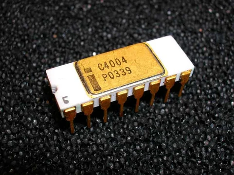
Microarchitecture
The implementation of an instruction set architecture in a processor.

NoahSPARC · CC0
Microarchitecture, sometimes called computer organization or shortened to μarch or uarch, describes how a specific processor implements a given instruction set architecture (ISA). Different microarchitectures can realize the same ISA, with variations arising from differing design goals or technological changes. Computer architecture itself is the combination of microarchitecture and the ISA.
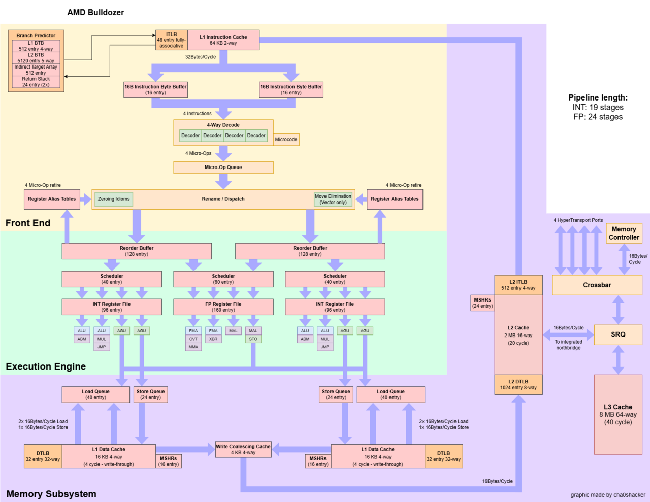
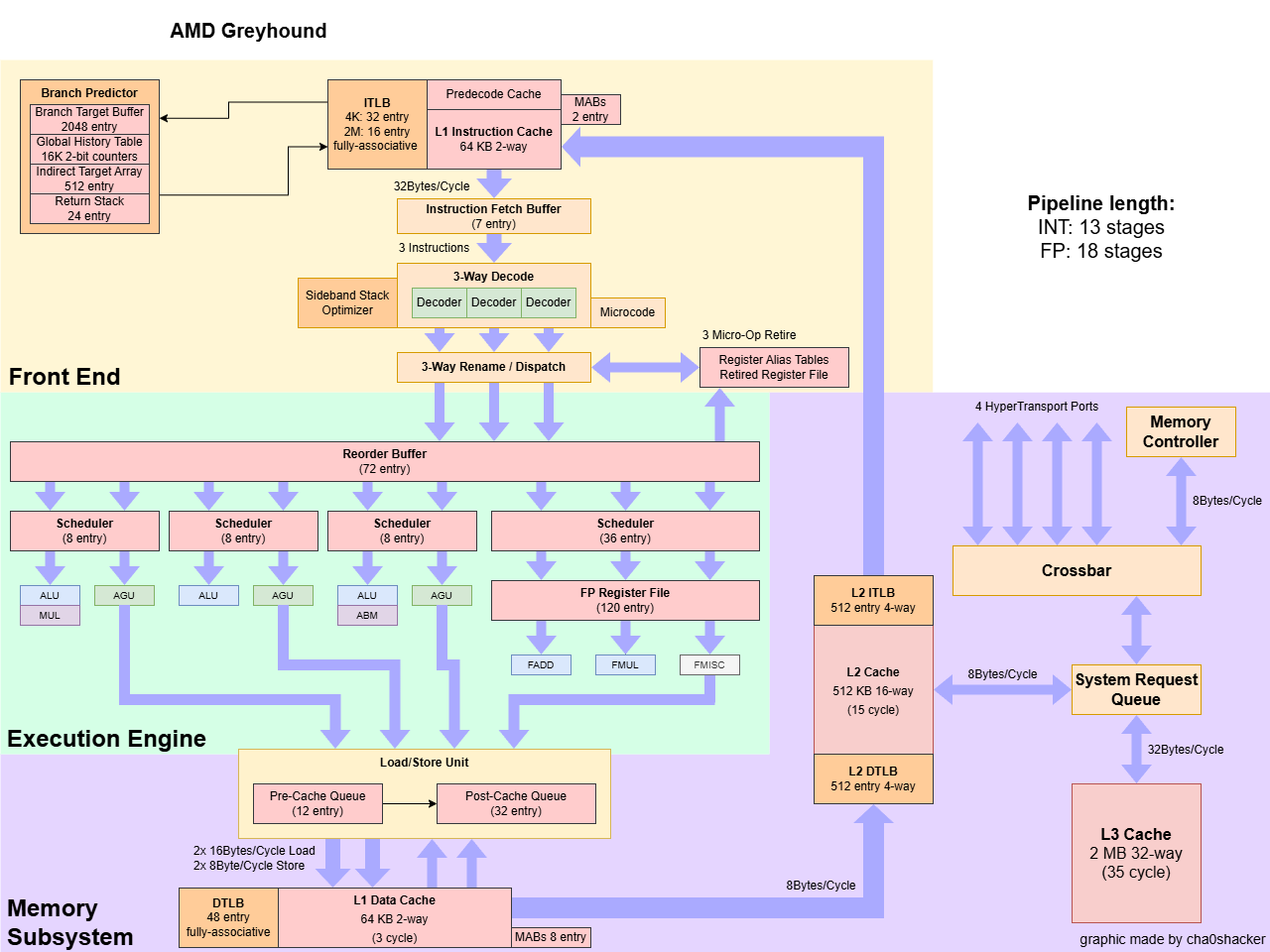
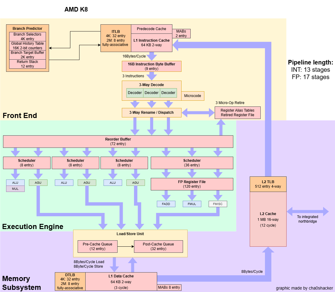
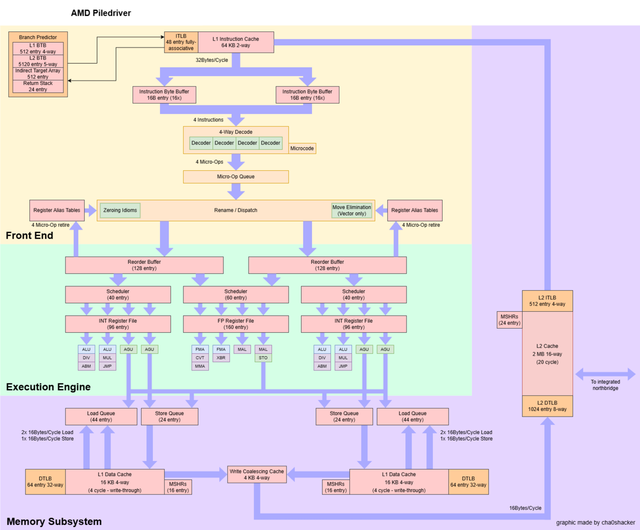
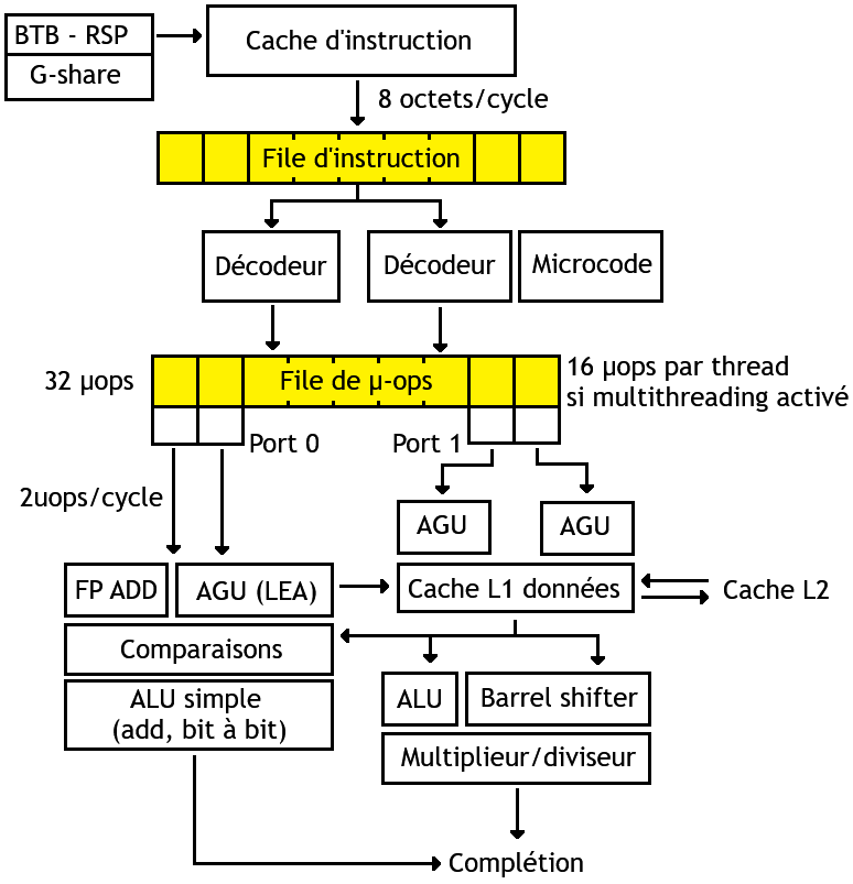
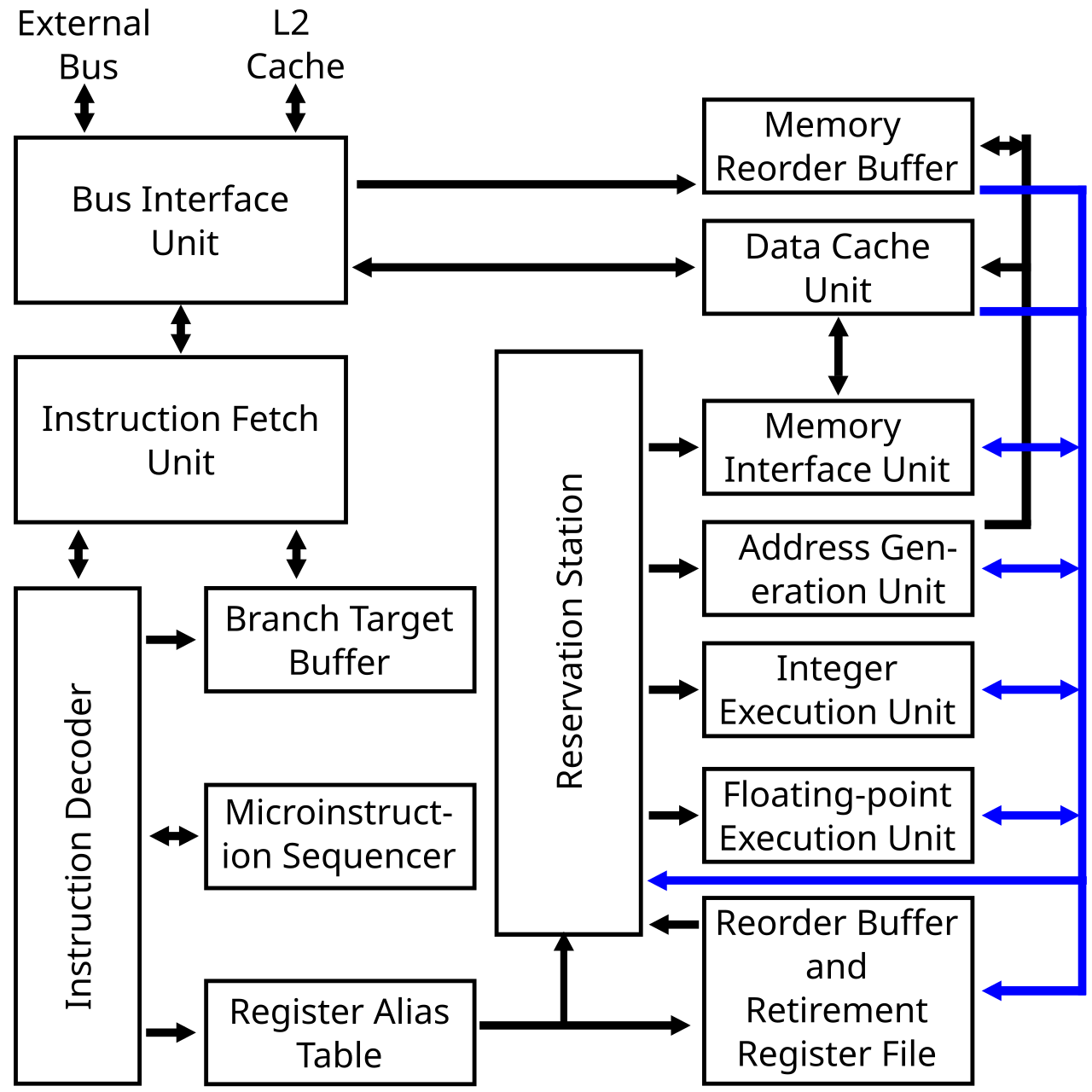
The ISA essentially defines the programming model visible to an assembly language programmer or compiler writer, covering instructions, execution model, registers, and data formats. Microarchitecture, in contrast, details the processor's internal components and how they connect and work together to carry out the ISA. It is typically shown in diagrams that map the interconnections of microarchitectural elements—ranging from individual gates and registers up to complete arithmetic logic units (ALUs) or larger blocks. These diagrams usually separate the datapath, where data moves, from the control path, which directs that movement.
Designers often draw the microarchitecture as a data flow diagram, similar to a block diagram. Symbols represent elements like the ALU or register file, and arrows—thick, thin, or otherwise—distinguish between three-state buses (requiring a three-state buffer for each driving device), unidirectional buses (driven by a single source, such as a memory address register), and individual control lines. Very simple computers might use a single three-state data bus, while more complex machines employ multiple three-state buses to perform more operations simultaneously. Each microarchitectural element is itself represented by a schematic of logic gates, and each gate by a circuit diagram of transistors in a particular logic family. Machines with different microarchitectures can share the same ISA, allowing them to run identical programs. New microarchitectures, circuit designs, and advances in semiconductor manufacturing enable newer processor generations to achieve higher performance while keeping the same ISA. In principle, a single microarchitecture could handle several different ISAs with only minor microcode changes.
The pipelined datapath is the most common design in modern microarchitecture, used in most microprocessors, microcontrollers, and DSPs.
- Also known as
- computer organization, μarch, uarch
- Relation to isa
- implements a given instruction set architecture
- Common representation
- diagrams showing datapath and control path
- Key design aspects
- pipelined datapath, execution units, memory hierarchy, system-level peripherals
- Design constraints
- chip area/cost, power consumption, logic complexity, ease of connectivity, manufacturability, ease of debugging, testability
Lore & Background
The earliest computers were multicycle designs, which execute the instruction cycle (read, decode, find data, process, write results) sequentially over several clock cycles. Multicycle architectures often use the least total number of logic elements and reasonable amounts of power, and they have no pipeline to stall when taking conditional branches or interrupts. However, other microarchitectures often perform more instructions per unit time using the same logic family.
Over time, the pipelined datapath became the most commonly used datapath design, allowing multiple instructions to overlap in execution like an assembly line. Pipeline stages typically include instruction fetch, instruction decode, execute, and write back, with some architectures adding a memory access stage. Execution units such as arithmetic logic units, floating point units, load/store units, branch prediction, and SIMD units perform the processor's operations.
The memory hierarchy—including caching, main memory, and non-volatile storage—has always been slower than the processor itself, introducing delays. A central goal has been to execute more instructions in parallel to increase effective execution speed, which introduced complicated logic and circuit structures. Initially these techniques were only feasible on expensive mainframes or supercomputers, but as semiconductor manufacturing progressed, more could be implemented on a single chip.
Reader's Guide
Microarchitecture is significant because it determines how an instruction set architecture is realized in hardware, directly affecting performance, power consumption, cost, and other constraints. The same ISA can be implemented with different microarchitectures, allowing newer generations of processors to achieve higher performance through improved microarchitectural and circuitry solutions, along with advances in semiconductor manufacturing. The design of pipelines, execution units, and memory systems are central microarchitectural tasks that shape a processor's capabilities.
Microarchitectural design pays close attention to constraints such as chip area, power consumption, logic complexity, ease of connectivity, manufacturability, debugging, and testability—unlike architectural design, where achieving a specific performance level is the main goal. The choice of instruction set architecture may greatly affect the complexity of implementing high-performance devices. The prominent strategy used to develop the first RISC processors was to simplify instructions to a minimum of individual semantic complexity combined with high encoding regularity and simplicity.
In principle, a single microarchitecture could execute several different ISAs with only minor changes to the microcode. The legacy of microarchitecture is that it enables the continuous improvement of processor performance while maintaining software compatibility with existing instruction sets.
Did You Know?
- The ISA is roughly the same as the programming model of a processor as seen by an assembly language programmer or compiler writer.
- The pipelined datapath is the most commonly used datapath design in microarchitecture today.
- Maurice Wilkes invented the tabular approach to control logic and called it microprogramming.
The Superscalar Breakthrough
The P5 Pentium marked a watershed moment in x86 history as the first processor in that family to execute two instructions simultaneously through a dual integer pipeline. This superscalar capability had long been considered by academics and RISC-focused competitors to be fundamentally incompatible with the complex CISC instruction set that defined the x86 architecture. Intel's Santa Clara design team, the same group behind the 386 and 486, chose a convergence strategy that blended RISC-like techniques with the existing CISC instruction set, leveraging both optimized microcode and direct execution depending on the particular instruction. Some implementation techniques drew from the earlier Intel i960 CA processor of 1989, while other elements were novel to the P5 design. The team also carried forward strategies from the i386 and i486 for handling the notoriously intricate x86 encodings within a pipelined execution model. To fully exploit the dual pipelines, Intel invested in working with compiler vendors, independent software developers, and operating system companies to optimize their products for instruction-level parallelism, though not every application saw substantial gains from recompilation.
The Long Road to Silicon
Design work on what would become the P5 microarchitecture began in June 1989, with the Santa Clara team settling on a superscalar RISC architecture merging RISC and CISC technology, incorporating on-chip cache, a floating-point unit, and branch prediction. Vinod Dham, then Vice President of the Microprocessor Product Group, championed bringing RISC technology into the existing x86 framework to compete in broader markets. The team set ambitious targets, aiming to boost the FPU by three to five times over the Intel486. The preliminary design was successfully simulated in 1990, after which layout work commenced with several dozen engineers. Pre-silicon verification demanded roughly 100 million clock cycles of testing, with major operating systems and applications booted and run. By late 1990, the planned features would not fit on the die, forcing a redesign to slim the circuit without sacrificing performance. Engineers ran hundreds of validation tests across 5,000 different variables, finding only a handful of bugs across 14 circuit boards. The design was taped out by February 1992, with beta-testing beginning in April. By mid-1992, the P5 team had grown to 200 engineers. Intel planned to demonstrate the chip at PC Expo in June 1992, but design problems forced the demo's cancellation.
Performance Architecture and Technical Features
The P5 Pentium packed a remarkable set of architectural enhancements that collectively transformed x86 performance. At its core sat a redesigned floating-point unit that Intel noted was ten times faster than the one in the i486, delivering a dramatic leap in floating-point throughput. The processor featured a wide 64-bit burst-mode data bus, both external and internal, alongside 256-bit internal data buses and write-back caches. Separate code and data caches further improved memory access efficiency. The chip also included System Management Mode, a feature inherited from Intel's earlier SL architecture. Perhaps most notably, the P5 introduced hardware support for multiprocessing, a capability absent in all prior x86 generations and in competing x86 processors. Intel collaborated with IBM to define this ability and integrate it into the P5 microarchitecture, drawing parallels to IBM mainframe computers. In terms of measured performance, the 66 MHz Pentium achieved 112 V1.1 Dhrystone MIPS, a SPECint92 rating of 64.5, a SPECfp92 rating of 56.9, and an iCOMP index of 567. The performance gap between the 60 MHz and 66 MHz variants was approximately 10 percent.
Legacy, Succession, and the Name
The Pentium name itself carries a story. Derived from the Greek word pente, meaning five, it referenced the fifth generation in Intel's numeric x86 naming convention spanning the 8086 through 80486, with the Latin suffix -ium added to avoid the awkward 80586. The P5 was introduced on March 22, 1993, as the first CPU to bear the Pentium brand. Its legacy extended well beyond its initial release. In November 1995, the P6-based Pentium Pro took over the workstation and server markets. In January 1997, the Pentium MMX arrived, layering the MMX instruction set, larger caches, and other enhancements onto the same P5 microarchitecture. The Pentium II brand then succeeded it at the top end, while P5-based processors continued as a low-end line until July 1999, when the Celeron brand, already having absorbed the 486 name, finally replaced them. At launch, the Pentium faced a crowded field of superscalar competitors, including the PowerPC 601, SuperSPARC, DEC Alpha 21064, AMD 29050, Motorola MC88110, and Motorola 68060, most of which also employed in-order dual instruction pipelines. The non-superscalar Motorola 68040 and MIPS R4000 rounded out the competitive landscape.
Gallery
Frequently Asked Questions
What exactly is microarchitecture?
Microarchitecture (also called computer organization, μarch, or uarch) is the specific way a particular processor chip carries out the instructions defined by its instruction set architecture. Think of it as the internal blueprint—the datapath, control logic, and execution units—that turns abstract ISA operations into real hardware behavior.
How does microarchitecture differ from the ISA?
The ISA is the programmer-facing contract: it specifies which instructions exist, what registers are available, and how data is formatted. Microarchitecture is the engineer's answer to 'how do we actually build that?'—two chips can speak the same ISA yet use entirely different internal pipelines, caches, and execution units to get the job done.
What are the key building blocks of a microarchitecture?
A typical microarchitecture diagram lays out the datapath and control path, and it generally includes a pipelined datapath, one or more execution units, a memory hierarchy, and system-level peripherals. These components are arranged to balance performance against practical limits.
Why can two processors implement the same ISA with different microarchitectures?
Designers make different trade-offs depending on their goals—mobile power efficiency versus desktop peak throughput, for example—so pipeline depth, cache sizing, and execution-unit layout will vary. Technological shifts such as new process nodes or memory technologies also push designers toward different organizational choices even when the ISA stays fixed.
What real-world constraints shape a microarchitecture?
Beyond raw performance, a chip's microarchitecture must fit within a target die area and cost, stay inside a power budget, keep logic complexity manageable, and be easy to connect to the rest of the system. Manufacturability, ease of debugging, and testability are equally critical practical considerations that influence every design decision.
More in Microprocessors 1-24
Spotted an error? Know more?
Reader corrections go straight into our review queue. Suggest an edit · How this site is sourced