
Gracemont (microarchitecture)
Fourth-generation out-of-order low-power Atom microarchitecture for hybrid processors.

Unknown author · Public domain
Gracemont is a low-power processor microarchitecture from Intel, designed for use in systems on a chip (SoCs). It follows Tremont and appears as the efficient cores in the hybrid designs of the Alder Lake, Raptor Lake, and Raptor Lake Refresh processors.
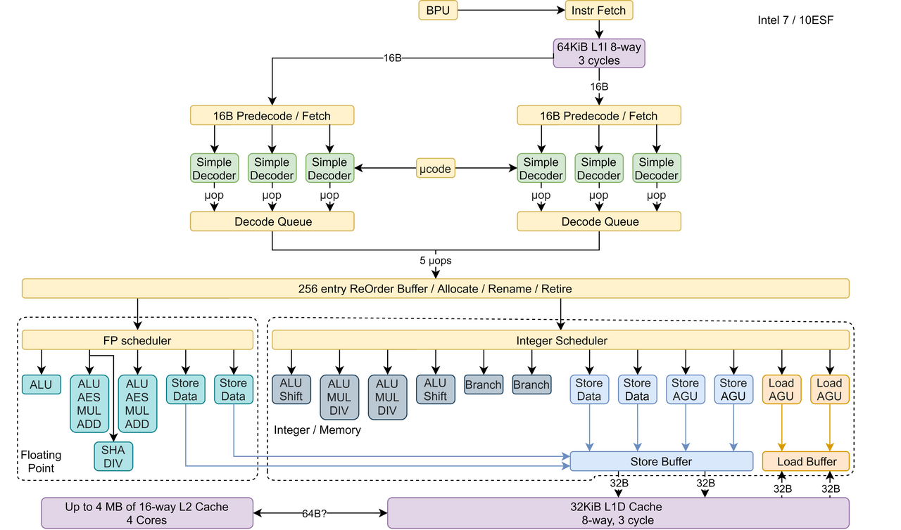
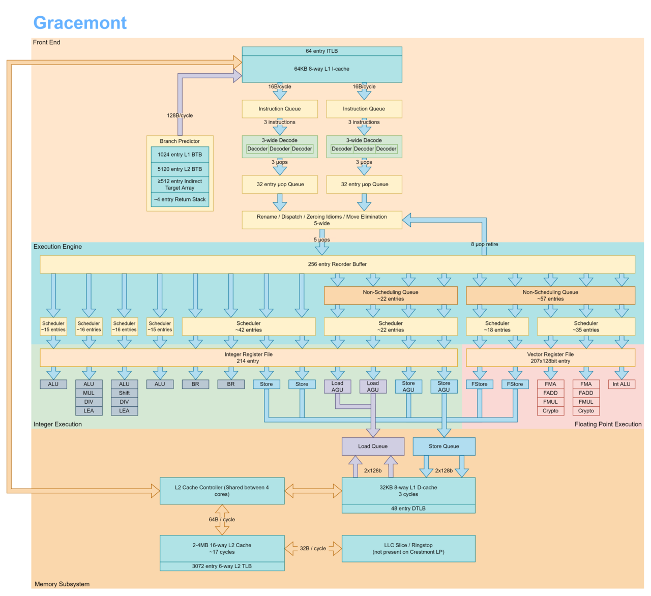
This microarchitecture represents the fourth generation of out-of-order, low-power Atom designs, fabricated on the Intel 7 process. Compared to Tremont, Gracemont brings several improvements. Each core gets an eight-way-associative 64 KB instruction cache and an eight-way-associative 32 KB data cache in its Level 1 cache. A new on-demand instruction-length decoder is included. The microarchitecture can issue up to five instructions per clock cycle (up from four) and retire up to eight per clock (up from seven). It features 17 execution ports (functional units), up from ten, and a reorder buffer expanded to 256 entries from 208. Branch prediction has been improved, and support is added for AVX, AVX2, FMA3, and AVX-VNNI instructions. The shared L2 cache per four-core cluster is either 2 MB or 4 MB: Alder Lake family chips have 2 MB; higher-end Raptor Lake family chips with Raptor Cove cores have 4 MB, while lower-end Raptor Lake family chips with Golden Cove cores have 2 MB.
The technology uses a system-on-a-chip (SoC) architecture with 3D tri-gate transistors. Thermal design power (TDP) ratings are 10 W for desktop processors and 6 W for mobile processors.
Gracemont serves as the efficient cores in Intel’s 12th-generation (Alder Lake), 13th-generation (Raptor Lake), and 14th-generation (Raptor Lake Refresh) hybrid Core processors. It is also used as the sole core cluster in the Alder Lake-N lineup, which targets low-power applications.
Quick Facts
- Produced-Start
- 2021-11-04
- Soldby
- Intel
- Cores
- 4 per module
- Slowest
- 0.7
- Slow-Unit
- GHz
- Fastest
- 4.3
- Arch
- x86-64
- Extensions
- MMX, SSE, SSE2, SSE3, SSSE3, SSE4.1, SSE4.2, AVX, AVX2, FMA3, AVX-VNNI, AES-NI, CLMUL, RDRAND, SHA, TXT, VT-d, VT-x
- Predecessor
- Tremont
Facts from the source article.
Lore & Background
Gracemont is the fourth generation out-of-order low-power Atom microarchitecture, built on the Intel 7 manufacturing process. It features enhancements over Tremont including a new on-demand instruction-length decoder, improved branch prediction, and support for AVX, AVX2, FMA3 and AVX-VNNI instructions. The microarchitecture uses 3D tri-gate transistors and is designed as a system on a chip (SoC).
The Gracemont microarchitecture is used as the efficient cores of the 12th generation of Intel Core hybrid processors (codenamed 'Alder Lake'), the 13th generation (codenamed 'Raptor Lake'), and the 14th generation (codenamed 'Raptor Lake Refresh'). It is also used in the Alder Lake-N line-up as the only core cluster, intended for low-power applications.
Thermal design power (TDP) ratings include 10W for desktop processors and 6W for mobile processors. The shared L2 cache per 4-core cluster is either 2MB or 4MB: Alder Lake family has 2MB, higher-end Raptor Lake family with Raptor Cove has 4MB, while lower-end Raptor Lake family with Golden Cove has 2MB.
Reader's Guide
Gracemont represents a significant step in Intel's hybrid processor strategy, serving as the low-power core in three generations of Core processors: Alder Lake, Raptor Lake, and Raptor Lake Refresh. Its inclusion in the Alder Lake-N line-up as the sole core cluster demonstrates its capability to function independently in low-power applications. The microarchitecture's enhancements over Tremont—such as increased instruction issue and retire rates, a larger reorder buffer, and additional execution ports—improve performance for power-constrained environments. Support for AVX, AVX2, FMA3, and AVX-VNNI instructions extends its computational capabilities. The variable L2 cache sizes (2MB or 4MB per 4-core cluster) depending on the processor family allow for differentiation between performance tiers. With TDP ratings of 10W for desktop and 6W for mobile, Gracemont is positioned for energy-efficient computing in hybrid architectures, balancing power consumption with throughput in both desktop and mobile contexts.
Did You Know?
- The microarchitecture has 17 execution ports, up from ten in Tremont.
- Alder Lake-N uses Gracemont as the only core cluster for low-power applications.
Mobile Roots and the Apple Connection
The Core brand entered the world on January 6, 2006, as an exclusively mobile offering built around the Yonah design. Derived from the Pentium M lineage rather than the Pentium 4 family, these 32-bit processors represented a deliberate return to the P6 microarchitecture tradition. The lineup split into two branches: the Core Duo, which placed two cores on a single die alongside a shared 2 MB L2 cache and an arbiter bus managing front-side bus access, and the Core Solo, which simply disabled one core on the same silicon to create a cheaper single-core option—a cost-saving trick Intel had employed before with the 486SX. Perhaps the most consequential partnership emerged from this launch: the Core Duo powered Apple's first-generation MacBook Pro, while the Core Solo found its way into the Mac Mini, marking the beginning of Apple's full transition to Intel silicon. Despite Intel's aggressive rebranding, some OEMs continued to label Yonah-based machines as Pentium M. By 2007, mainstream mobile Yonah chips were rebranded as Pentium Dual-Core, and by early 2008, several Core-branded SKUs had been discontinued.
Conroe and the Desktop Debut
Six months after the mobile-only Core launch, Intel brought the brand to desktops in July 2006 with the Core 2 series, headlined by the Conroe design. Built on a 65-nanometer process, Conroe was a dual-core chip that introduced 64-bit support and, in later iterations, scaled to four cores. What made Conroe remarkable was not raw clock speed but efficiency: it delivered performance that matched or exceeded the Pentium 4 across nearly every benchmark while running at dramatically lower frequencies. This was achieved through a deeply pipelined, resource-rich out-of-order execution engine that maintained high instructions-per-cycle throughput—a design philosophy that became a defining trait of the entire Core family going forward. The Core 2 also displaced the Pentium brand from the mid-to-high-end segment, pushing Pentium down into the budget tier. Identical or more capable variants of these processors were simultaneously sold under the Xeon name for workstation and server applications. The Core 2 thus established the template: a multi-core, high-IPC architecture that prioritized efficiency over brute clock rates, a principle that would guide Intel's Core line for nearly two decades.
Architectural Evolution and the Product Ladder
After Conroe set the baseline, Intel's subsequent Core generations favored incremental additions over wholesale redesigns. The most significant leap came in November 2008 with the 45-nanometer Bloomfield processor on the Nehalem architecture, which overhauled I/O and memory subsystems by introducing the QuickPath Interconnect and an integrated memory controller capable of driving up to three channels of DDR3. Sandy Bridge, arriving in January 2011 on a 32-nanometer process, added the Advanced Vector Extensions instruction set, while later generations brought deeper virtualization support and expanded management features through the ongoing refinement of Intel Active Management Technology. Alongside these architectural steps, Intel built out a tiered product ladder: Core i7 debuted in 2008, i5 followed in 2009, i3 in 2010, and the enthusiast-oriented i9 arrived in 2017. By that point the Core brand spanned four distinct lines targeting entry-level, mainstream, high-end, and enthusiast segments, all sharing the common DNA of multi-core design and high IPC that Conroe had established nearly a decade earlier.
Dropping the 'i': The 2023 Rebrand
In June 2023, Intel announced a significant simplification of its Core branding: the letter 'i' would be retired entirely. The mid-range through high-end processors previously known as Core i3, i5, i7, and i9, manufactured from 2008 to 2024, would simply become Core 3, Core 5, and Core 7. For the super-high-end tier, a new 'Ultra' designation was introduced, yielding Core Ultra 5, Core Ultra 7, and Core Ultra 9. The revised naming scheme made its first appearance with the Raptor Lake-U Refresh and Meteor Lake processors in 2024, where Core 3/5/7 covered mainstream desktop and laptop offerings while the Core Ultra line occupied the premium segment. This rebrand completed a long arc that began in 2006, when a mobile-only 32-bit dual-core chip first carried the Core name. The Pentium brand, displaced from the upper market by Core's arrival, now occupies the entry-level and budget space, while Xeon continues to serve server and workstation customers with functionally equivalent or enhanced silicon.
Gallery
Frequently Asked Questions
Who is Gracemont (microarchitecture)?
Gracemont is Intel's fourth-generation out-of-order, low-power Atom microarchitecture, built specifically to serve as the efficient-core (E-core) inside hybrid SoC designs. It is the direct successor to Tremont and is fabricated on the Intel 7 process node.
What are Gracemont (microarchitecture)'s powers and role?
In Alder Lake, Raptor Lake, and Raptor Lake Refresh, Gracemont cores handle background and low-priority workloads at minimal energy draw while the performance cores tackle heavy tasks. Each core issues five instructions per clock and retires up to eight, backed by 17 execution ports.
Why is Gracemont (microarchitecture) important?
It is the architectural backbone of Intel's hybrid CPU strategy, allowing a single die to blend high-throughput P-cores with ultra-efficient E-cores for better performance-per-watt. Without Gracemont, the multi-core hybrid designs of Alder Lake and its successors would lack their low-power half.
What are Gracemont (microarchitecture)'s key specs compared to Tremont?
Gracemont upgrades the L1 cache to a 64 KB eight-way-associative instruction cache and a 32 KB eight-way-associative data cache per core, both larger than its predecessor. It also widens the issue and retire pipelines to 5-wide and 8-wide respectively, while being manufactured on the Intel 7 node.
More in Intel and AMD Microprocessors, Part 2 1-24
Spotted an error? Know more?
Reader corrections go straight into our review queue. Suggest an edit · How this site is sourced