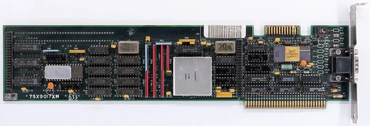
Intel Graphics Technology
Integrated graphics built into Intel CPUs since 2010.

Intel Graphics Technology (GT) is a family of integrated graphics processors (IGPs) that Intel designs and manufactures itself, with some units also produced under contract by TSMC. These GPUs sit on the same chip as the CPU and are standard in most Intel-powered desktops and laptops. The line debuted in 2010 under the name Intel HD Graphics, was rebranded as Intel UHD Graphics in 2017, and replaced the older Graphics Media Accelerator (GMA) series. Starting in 2013, Intel also released more powerful versions under the Iris, Iris Pro, and Iris Plus labels, which pack more execution units and, in certain models, embedded memory (eDRAM). Intel Graphics Technology coexists with Intel Arc, the company’s discrete graphics card lineup for gaming and high-performance tasks.
Before HD Graphics arrived, Intel’s integrated graphics lived on the motherboard’s northbridge as part of the Hub Architecture, going by names like Intel Extreme Graphics and Intel GMA. When Intel shifted to the Platform Controller Hub (PCH) design, the northbridge disappeared, and graphics processing moved onto the same die as the CPU. The earlier GMA series had a poor reputation for performance and features, making it unsuitable for demanding graphics work like 3D gaming. The performance boost from HD Graphics made Intel’s offerings competitive with integrated graphics from rivals Nvidia and ATI/AMD.
Intel’s HD and Iris Graphics are organized into generations, each split into performance tiers labeled with a “GTx” designation. Every generation corresponds to a Gen graphics microarchitecture and its associated GEN instruction set architecture, starting with Gen4.
The Gen5 architecture arrived in January 2010 with Clarkdale and Arrandale processors, which featured Ironlake graphics branded as Celeron, Pentium, or Core with HD Graphics. These had a single specification: 12 execution units, topping out at 43.2 GFLOPS at 900 MHz, and could decode H.264 1080p video at up to 40 fps. Its direct predecessor, the GMA X4500, had 10 EUs at 800 MHz but lacked some capabilities.
Gen6 came with Sandy Bridge processors in January 2011, introducing “second generation” HD Graphics. Sandy Bridge Celeron and Pentium chips got Intel HD, while Core i3 and above offered either HD 2000 or HD 3000, both with hardware video encoding and HD postprocessing effects.
Quick Facts
- Created
- 2010
- Openglversion
- 2.1+ (Depending on version, see capabilities)
- Openclversion
- 1.2+ (Depending on version, see capabilities)
- Vulkanapi
- 1.4+ (Depending on version, see capabilities)
- Predecessor
- Intel GMA
- Successor
- Intel Xe
- Designfirm
- Intel
- Support Status
- Supported
- Manufacturer
- Intel and TSMC
Facts from the source article.
Lore & Background
Before Intel HD Graphics, Intel integrated graphics were built into the motherboard's northbridge as part of the Intel Hub Architecture, known as Intel Extreme Graphics and Intel GMA. With the Platform Controller Hub design, the northbridge was eliminated and graphics processing moved to the same die as the CPU. The previous GMA series had a reputation for lacking performance and features, not considered good for demanding applications like 3D gaming. The performance increases of HD Graphics made the products competitive with integrated graphics from Nvidia and ATI/AMD.
Intel HD and Iris Graphics are divided into generations, each corresponding to a Gen graphics microarchitecture with a GEN instruction set architecture since Gen4. Within each generation are tiers of increasing performance, denominated by the 'GTx' label. The Gen5 architecture (Westmere, January 2010) featured 12 execution units and up to 43.2 GFLOPS. Gen6 (Sandy Bridge, January 2011) introduced hardware video encoding and HD postprocessing. Gen7 (Ivy Bridge, April 2012) added HD 2500 and HD 4000 tiers. Gen7.5 (Haswell, June 2013) introduced four tiers including Iris Pro GT3e with 128 MB of eDRAM (Crystalwell) as a Level 4 cache. Gen8 (Broadwell) continued Iris Pro for desktop enthusiasts. Gen9 (Skylake, August 2015) retired VGA support and added Vulkan 1.3 and DirectX 12 Feature Level 12_2. Gen9.5 (Kaby Lake, August 2016) added 4K UHD DRM streaming and HEVC/VP9 decode. Gen11 (Ice Lake) introduced 10 nm Gen 11 GPU microarchitecture with variable rate shading and integer scaling. Xe-LP architecture (Gen12) added AV1 hardware decoding and removed FP64 support. Arc Alchemist Tile GPU (Gen12.7) added DirectX 12 Ultimate and 8K AV1 hardware encoding.
Reader's Guide
Intel Graphics Technology is notable as the integrated graphics solution that replaced the earlier GMA series, moving graphics processing from the motherboard northbridge onto the CPU die. This integration, beginning in 2010 with Intel HD Graphics, made graphics capabilities standard in most Intel-based desktops and laptops. The series evolved through multiple generations, each introducing new features: hardware video encoding with Sandy Bridge, eDRAM cache with Haswell's Iris Pro, Vulkan and DirectX 12 support with Skylake, and AV1 hardware decoding with Xe-LP. The higher-performance Iris, Iris Pro, and Iris Plus brands, introduced in 2013, targeted users needing more graphics power. Intel Graphics Technology is sold alongside Intel Arc, the company's discrete graphics cards for gaming and high-performance applications. The series' legacy includes making integrated graphics competitive with rivals Nvidia and ATI/AMD, and supporting virtualization technologies like GVT-d, GVT-s, GVT-g, and SR-IOV across various generations.
Did You Know?
- Intel HD Graphics was introduced in 2010, renamed Intel UHD Graphics in 2017.
- The Iris Pro GT3e in Haswell CPUs included 128 MB of eDRAM as a Level 4 cache called Crystalwell.
- Intel Quick Sync Video, a hardware video encoding and decoding technology, was introduced with Sandy Bridge in January 2011.
From Northbridge to Die: The Architectural Shift
Before 2010, Intel's integrated graphics resided on the motherboard's northbridge chip as part of the company's Hub Architecture, marketed under the Extreme Graphics and GMA names. That GMA line carried a well-known reputation for weak performance and missing features, making it a poor fit for demanding tasks such as 3D gaming. The Platform Controller Hub redesign eliminated the northbridge altogether and relocated graphics processing onto the same silicon die as the CPU. This structural change set the stage for the January 2010 launch of Intel HD Graphics on Clarkdale and Arrandale processors, which shipped with 12 execution units and up to 43.2 GFLOPS at 900 MHz. Moving from a separate chipset component to a unified processor package fundamentally altered how integrated graphics could scale, and it established the architectural foundation that every subsequent generation—from Sandy Bridge and Ivy Bridge through the Xe-LP and Arc Alchemist Tile microarchitectures—has built upon.
Tiers, Brands, and the Iris Line
Intel organizes its integrated GPU lineup into discrete generations, each tied to a specific microarchitecture and a corresponding instruction set that has been tracked since Gen4. Within every generation, performance is stratified into tiers identified by GTx labels, allowing the company to differentiate budget Celeron and Pentium parts from higher-end Core offerings. Beginning in 2013, Intel introduced higher-performance variants under the Iris, Iris Pro, and Iris Plus brands, which added more execution units and, in select models, embedded memory. The Haswell-generation Iris Pro GT3e, for instance, carried 128 MB of eDRAM on a separate die within the same package, which Intel designated as a Level 4 cache shared between CPU and GPU and branded Crystalwell. This tiered approach lets Intel serve the full spectrum from entry-level machines to enthusiast Broadwell-K desktops, all while keeping the integrated line distinct from the company's separate Intel Arc discrete graphics cards aimed at gaming and high-performance workloads.
Media Engine and Display Evolution
A defining thread through Intel's integrated graphics history is the steady expansion of its media and display capabilities. Sandy Bridge and Ivy Bridge generations introduced hardware video encoding and HD postprocessing effects. Skylake retired legacy VGA support and enabled up to three simultaneous monitors over HDMI 1.4, DisplayPort 1.2, or eDP 1.3 interfaces. Kaby Lake added full hardware acceleration for 8- and 10-bit HEVC and VP9 decode alongside 4K UHD premium streaming. Later generations pushed further still: Ice Lake brought dual HEVC 10-bit encode pipelines, three 4K display outputs, variable rate shading, and integer scaling. The Xe-LP (Gen12) generation added AV1 8-bit and 10-bit fixed-function hardware decoding, while the Arc Alchemist Tile GPU found in Meteor Lake and Arrow Lake introduced an 8K 10-bit AV1 hardware encoder and native HDMI 2.1 at 48 Gbps. Each successive step reflects Intel's strategy of embedding professional-grade media handling directly into mainstream processors rather than leaving it to add-on cards.
Competitive Context and the Broader Ecosystem
The GMA series had long been regarded as inadequate for graphics-intensive work, leaving a gap that rivals Nvidia and ATI/AMD filled with their own integrated adapters. Intel HD Graphics closed much of that gap, making the company's integrated options genuinely competitive in the mid-2010s. Intel now operates a two-pronged graphics strategy: the integrated GT line, rebranded Intel UHD Graphics in 2017, ships inside virtually every Intel-based desktop and laptop, while the Intel Arc line of discrete graphics cards targets gaming and high-performance applications. Manufacturing is split between Intel's own fabs and contract production at TSMC. Software support spans Vulkan 1.3 (extending to 1.4 via Mesa), DirectX 12 Feature Level 12_2, and, on newer Xe-LP and Arc Alchemist Tile parts, DirectX 12 Ultimate. This dual approach lets Intel address the full spectrum from everyday computing to creative and gaming workloads without relying on a single product category.
Frequently Asked Questions
What is Intel Graphics Technology?
Intel Graphics Technology refers to the line of integrated graphics processors that Intel designs and builds directly onto its own CPU chips. These IGP units ship as standard in the vast majority of Intel-based desktops and laptops, with some production handled by TSMC under contract.
When did the Intel Graphics Technology line debut?
The family first appeared in 2010 under the Intel HD Graphics name, stepping in to replace the earlier Graphics Media Accelerator (GMA) series. In 2017, Intel rebranded the standard tier as Intel UHD Graphics.
What are Iris, Iris Pro, and Iris Plus?
Introduced in 2013, these are the higher-performance variants within the Intel GT lineup that carry a greater number of execution units than the base HD or UHD chips. They target users who need more graphical muscle without resorting to a discrete GPU.
How much performance does a Gen5 Intel GPU deliver?
The fifth-generation Intel graphics part tops out at 43.2 GFLOPS when running at its 900 MHz clock speed. It features 12 execution units, a meaningful step up from the GMA-era predecessors it replaced.
Why does Intel's integrated graphics matter to the broader market?
Because the GPU lives on the same die as the CPU, virtually every Intel-powered machine gets usable graphics out of the box without a separate graphics card. This makes it the default visual output for the largest installed base of personal computers worldwide.
More in Graphics Hardware, Part 2 1-24
Spotted an error? Know more?
Reader corrections go straight into our review queue. Suggest an edit · How this site is sourced