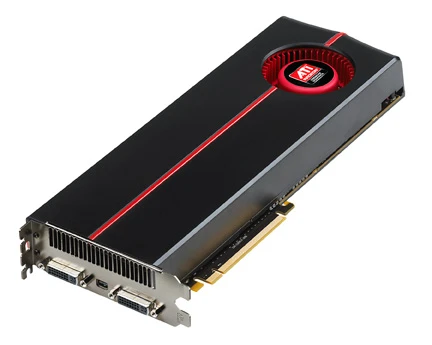
ULTRAY2000
Concept GPU with fixed and programmable pipeline, MAESTRO technology.

The ULTRAY2000 was a concept chip for real-time 3D graphics processing, created by the Japanese GPU design firm Digital Media Professionals Inc. (DMP). Manufactured using TSMC’s 0.13 μm process, it packed over 100 million CMOS transistors and ran its GPU core at 200 MHz, with an integrated memory controller supporting DDR-400 memory. DMP announced the chip on July 21, 2005, and first showed it at SIGGRAPH 2005, with initial sample shipments planned for fall of that year. Its architecture combined a fixed graphics pipeline with an advanced instruction programmable core. The chip also included hardware-specific features called “MAESTRO” technology, which embedded modeled algorithms for generating physical light reflection and shadow properties for various materials, enabling realistic 3D graphics at high resolution in real time. The ULTRAY2000 was succeeded by the PICA200.
At SIGGRAPH 2005, the public exhibition card ran at a 200 MHz core clock on a 130 nm TSMC process, with 256 MB of DDR-400 SDRAM on a 256-bit memory bus, yielding 12.8 GB/s of memory bandwidth. It used a PCI bus supporting both 64-bit/66 MHz and 32-bit/33 MHz cards. Display outputs included digital DVI-I and analog RGB Dsub-15 connectors, but only one display could be connected at a time. The chip supported OpenGL 2.0, OpenGL ES 2.0, and Java Mobile 3D Graphics for J2ME (JSR-000184), later known as M3G 1.0/1.1 from 2007. The exhibited part did not support PCI Express due to high licensing fees, as the project’s main business plan targeted embedded platforms.
DMP’s “MAESTRO” technology modeled various computer graphics algorithms for later hardware implementation on proprietary solutions, allowing custom graphics features to be built into silicon.
- Manufacturer
- Digital Media Professionals Inc. (DMP)
- Announced
- July 21, 2005
- First exhibition
- SIGGRAPH 2005
- Process technology
- 0.13 μm TSMC
- Transistor count
- More than 100 million CMOS transistors
- Core clock
- 200 MHz
- Memory support
- DDR-400 SDRAM (256 MB on 256-bit bus, 12.8 GB/s bandwidth)
- Apis supported
- OpenGL 2.0, OpenGL ES 2.0, Java Mobile 3D Graphics for J2ME (M3G 1.0/1.1)
Lore & Background
The ULTRAY2000 was announced by DMP on July 21, 2005, and first exhibited at SIGGRAPH 2005. The first sample shipments were scheduled for the fall of 2005. It was produced in a 0.13 μm TSMC manufacturing process and contained more than 100 million CMOS transistors, with a GPU core clock running at 200 MHz and an integrated memory controller supporting DDR-400 memory. The exhibited part at SIGGRAPH 2005 used a PCI interface bus supporting both 64-bit/66 MHz and 32-bit/33 MHz cards, and did not support PCI Express due to high licensing fees, as the project's main business plan was focused on embedded platforms.
The chip adopted a design where a fixed graphics pipeline architecture coexists with an advanced instruction programmable core. It featured proprietary modeled algorithms for generating physical light reflection and shadow properties for various materials, embedded on the visual processor chip as hardware-specific features under the name 'MAESTRO' technology. This gave the chip the ability to process real-life looking 3D graphics at high resolution in real time. The ULTRAY2000 was succeeded by the PICA200.
Reader's Guide
The ULTRAY2000 is significant as a concept chip that demonstrated DMP's MAESTRO technology, a set of hardware-implemented graphics algorithms for realistic rendering. The MAESTRO technology included Shading Maestro (BRDF, subsurface scattering), Figure Maestro (geometry processing and tessellation), Shadow Maestro (shadow map generation and filtering for soft-edged shadows), Particle Maestro (rendering fuzzy objects like clouds and smoke), and Glare Maestro (lens flare and glare textures). A later refinement, MAESTRO-2G, focused on higher resolutions by reducing processing content size and memory bandwidth usage, and added Mapping Maestro for texture mapping and procedural texturing while removing Glare Maestro support.
The chip's legacy lies in its focus on embedded platforms, as indicated by its support for OpenGL ES 2.0 and Java Mobile 3D Graphics (M3G) APIs, and its avoidance of PCI Express due to licensing costs. The ULTRAY2000 was succeeded by the PICA200, suggesting it served as a precursor to DMP's later embedded GPU designs. Its combination of fixed and programmable pipelines and hardware-accelerated material rendering was notable for real-time 3D graphics at the time.
Did You Know?
- It contained more than 100 million CMOS transistors and was produced in a 0.13 μm TSMC process.
- The exhibited part used a PCI bus, not PCI Express, due to high licensing fees.
- It featured MAESTRO technology, including Shading Maestro, Figure Maestro, Shadow Maestro, Particle Maestro, and Glare Maestro.
More in Graphics Hardware 1-24
Spotted an error? Know more?
Reader corrections go straight into our review queue. Suggest an edit · How this site is sourced